- 您现在的位置:买卖IC网 > PDF目录67985 > MCIMX534AVV8C (FREESCALE SEMICONDUCTOR INC) 32-BIT, 800 MHz, RISC PROCESSOR, PBGA529 PDF资料下载
参数资料
| 型号: | MCIMX534AVV8C |
| 厂商: | FREESCALE SEMICONDUCTOR INC |
| 元件分类: | 微控制器/微处理器 |
| 英文描述: | 32-BIT, 800 MHz, RISC PROCESSOR, PBGA529 |
| 封装: | 19 X 19 MM, 0.80 MM PITCH, ROHS COMPLIANT, PLASTIC, TEPBGA-529 |
| 文件页数: | 41/178页 |
| 文件大小: | 4711K |
| 代理商: | MCIMX534AVV8C |
第1页第2页第3页第4页第5页第6页第7页第8页第9页第10页第11页第12页第13页第14页第15页第16页第17页第18页第19页第20页第21页第22页第23页第24页第25页第26页第27页第28页第29页第30页第31页第32页第33页第34页第35页第36页第37页第38页第39页第40页当前第41页第42页第43页第44页第45页第46页第47页第48页第49页第50页第51页第52页第53页第54页第55页第56页第57页第58页第59页第60页第61页第62页第63页第64页第65页第66页第67页第68页第69页第70页第71页第72页第73页第74页第75页第76页第77页第78页第79页第80页第81页第82页第83页第84页第85页第86页第87页第88页第89页第90页第91页第92页第93页第94页第95页第96页第97页第98页第99页第100页第101页第102页第103页第104页第105页第106页第107页第108页第109页第110页第111页第112页第113页第114页第115页第116页第117页第118页第119页第120页第121页第122页第123页第124页第125页第126页第127页第128页第129页第130页第131页第132页第133页第134页第135页第136页第137页第138页第139页第140页第141页第142页第143页第144页第145页第146页第147页第148页第149页第150页第151页第152页第153页第154页第155页第156页第157页第158页第159页第160页第161页第162页第163页第164页第165页第166页第167页第168页第169页第170页第171页第172页第173页第174页第175页第176页第177页第178页
Electrical Characteristics
i.MX53xA Automotive and Infotainment Applications Processors, Rev. 3
Freescale Semiconductor
135
NOTE
All the timings for the SSI are given for a non-inverted serial clock
polarity (TSCKP/RSCKP = 0) and a non-inverted frame sync
(TFSI/RFSI = 0). If the polarity of the clock and/or the frame sync have
been inverted, all the timing remains valid by inverting the clock signal
STCK/SRCK and/or the frame sync STFS/SRFS shown in the tables
and in the figures.
All timings are on Audiomux Pads when SSI is being used for data
transfer.
“Tx” and “Rx” refer to the Transmit and Receive sections of the SSI.
The terms WL and BL refer to Word Length (WL) and Bit Length (BL).
For internal Frame Sync operation using external clock, the FS timing is
same as that of Tx Data (for example, during AC97 mode of operation).
4.7.18
UART I/O Configuration and Timing Parameters
4.7.18.1
UART RS-232 I/O Configuration in Different Modes
The i.MX53xA UART interfaces can serve both as DTE or DCE device. This can be configured by the
DCEDTE control bit (default 0 – DCE mode). Table 88 shows the UART I/O configuration based on the
enabled mode.
4.7.18.2
UART RS-232 Serial Mode Timing
The following sections describe the electrical information of the UART module in the RS-232 mode.
4.7.18.2.1
UART Transmitter
Figure 87 depicts the transmit timing of UART in the RS-232 serial mode, with 8 data bit/1 stop bit format.
Table 89 lists the UART RS-232 serial mode transmit timing characteristics.
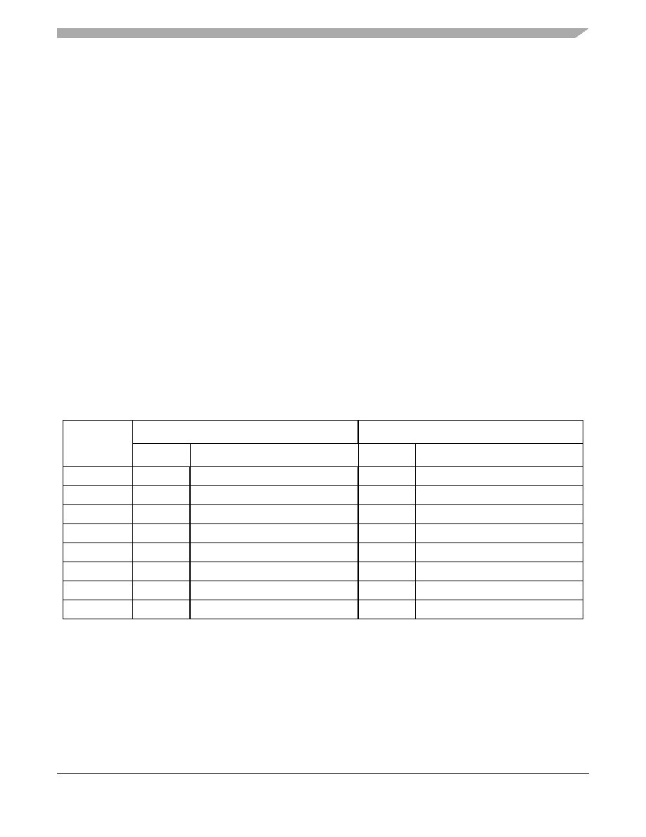
Table 88. UART I/O Configuration vs. Mode
Port
DTE Mode
DCE Mode
Direction
Description
Direction
Description
RTS
Output
RTS from DTE to DCE
Input
RTS from DTE to DCE
CTS
Input
CTS from DCE to DTE
Output
CTS from DCE to DTE
DTR
Output
DTR from DTE to DCE
Input
DTR from DTE to DCE
DSR
Input
DSR from DCE to DTE
Output
DSR from DCE to DTE
DCD
Input
DCD from DCE to DTE
Output
DCD from DCE to DTE
RI
Input
RING from DCE to DTE
Output
RING from DCE to DTE
TXD_MUX
Input
Serial data from DCE to DTE
Output
Serial data from DCE to DTE
RXD_MUX
Output
Serial data from DTE to DCE
Input
Serial data from DTE to DCE
相关PDF资料 |
PDF描述 |
|---|---|
| MCP23008T-E/SO | 8 I/O, PIA-GENERAL PURPOSE, PDSO18 |
| MCP23008-E/ML | 8 I/O, PIA-GENERAL PURPOSE, PQCC20 |
| MCP23S08T-E/ML | 8 I/O, PIA-GENERAL PURPOSE, PQCC20 |
| MCP23S08T-E/SS | 8 I/O, PIA-GENERAL PURPOSE, PDSO20 |
| MCP23008-E/P | 8 I/O, PIA-GENERAL PURPOSE, PDIP18 |
相关代理商/技术参数 |
参数描述 |
|---|---|
| MCIMX534AVV8C | 制造商:Freescale Semiconductor 功能描述:IC 32-BIT MPU 800 MHZ 529-BGA |
| MCIMX534AVV8CR2 | 功能描述:处理器 - 专门应用 iMX53 Rev 2.1 Auto RoHS:否 制造商:Freescale Semiconductor 类型:Multimedia Applications 核心:ARM Cortex A9 处理器系列:i.MX6 数据总线宽度:32 bit 最大时钟频率:1 GHz 指令/数据缓存: 数据 RAM 大小:128 KB 数据 ROM 大小: 工作电源电压: 最大工作温度:+ 95 C 安装风格:SMD/SMT 封装 / 箱体:MAPBGA-432 |
| MCIMX535DVV1B | 功能描述:处理器 - 专门应用 IMX53 REV 2.0 COMM RoHS:否 制造商:Freescale Semiconductor 类型:Multimedia Applications 核心:ARM Cortex A9 处理器系列:i.MX6 数据总线宽度:32 bit 最大时钟频率:1 GHz 指令/数据缓存: 数据 RAM 大小:128 KB 数据 ROM 大小: 工作电源电压: 最大工作温度:+ 95 C 安装风格:SMD/SMT 封装 / 箱体:MAPBGA-432 |
| MCIMX535DVV1C | 功能描述:处理器 - 专门应用 IMX53 REV 2.1 COMM RoHS:否 制造商:Freescale Semiconductor 类型:Multimedia Applications 核心:ARM Cortex A9 处理器系列:i.MX6 数据总线宽度:32 bit 最大时钟频率:1 GHz 指令/数据缓存: 数据 RAM 大小:128 KB 数据 ROM 大小: 工作电源电压: 最大工作温度:+ 95 C 安装风格:SMD/SMT 封装 / 箱体:MAPBGA-432 |
| MCIMX535DVV1C | 制造商:Freescale Semiconductor 功能描述:IMX53 REV 2.1 COMM |
发布紧急采购,3分钟左右您将得到回复。