- 您现在的位置:买卖IC网 > PDF目录2159 > MCP6N11T-100E/SN (Microchip Technology)IC AMP INSTR RRIO 35MHZ 8SOIC PDF资料下载
参数资料
| 型号: | MCP6N11T-100E/SN |
| 厂商: | Microchip Technology |
| 文件页数: | 21/50页 |
| 文件大小: | 0K |
| 描述: | IC AMP INSTR RRIO 35MHZ 8SOIC |
| 标准包装: | 3,300 |
| 放大器类型: | 仪表 |
| 电路数: | 1 |
| 输出类型: | 满摆幅 |
| 转换速率: | 6 V/µs |
| 增益带宽积: | 35MHz |
| 电流 - 输入偏压: | 10pA |
| 电压 - 输入偏移: | 350µV |
| 电流 - 电源: | 800µA |
| 电流 - 输出 / 通道: | 30mA |
| 电压 - 电源,单路/双路(±): | 1.8 V ~ 5.5 V |
| 工作温度: | -40°C ~ 125°C |
| 安装类型: | 表面贴装 |
| 封装/外壳: | 8-SOIC(0.154",3.90mm 宽) |
| 供应商设备封装: | 8-SOICN |
| 包装: | 带卷 (TR) |
第1页第2页第3页第4页第5页第6页第7页第8页第9页第10页第11页第12页第13页第14页第15页第16页第17页第18页第19页第20页当前第21页第22页第23页第24页第25页第26页第27页第28页第29页第30页第31页第32页第33页第34页第35页第36页第37页第38页第39页第40页第41页第42页第43页第44页第45页第46页第47页第48页第49页第50页
MCP6N11
DS25073A-page 28
2011 Microchip Technology Inc.
4.1.3
DC ERRORS
defines some of the DC error specifications. These
errors are internal to the INA, and can be summarized
as follows:
EQUATION 4-5:
The non-linearity specs (INLCM and INLDM) describe
errors that are non-linear functions of VCM and VDM,
respectively. They give the maximum excursion from
linear response over the entire common mode and
differential ranges.
The input bias current and offset current specs (IB and
IOS), together with a circuit’s external input resistances,
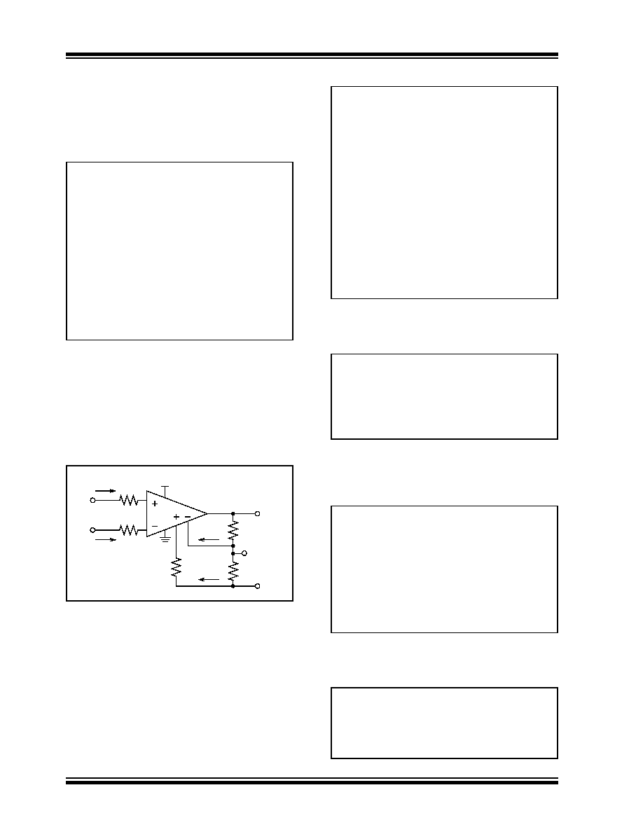
give an additional DC error. Figure 4-3 shows the
resistors that set the DC bias point.
FIGURE 4-3:
DC Bias Resistors.
The resistors at the main input (RIP and RIM) and its
input bias currents (IBP and IBM) give the following
changes in the INA’s bias voltages:
EQUATION 4-6:
The best design results when RIP and RIM are equal
and small:
EQUATION 4-7:
The resistors at the feedback input (RR, RF and RG)
and its input bias currents (IBR and IBF) give the
following changes in the INA’s bias voltages:
EQUATION 4-8:
The best design results when GDMRR and RF are equal
and small:
EQUATION 4-9:
Where:
V
OUT
V
REF
G
DM 1gE
+
() V
DM
ΔV
ED
+
()
+
=
G
DM 1gE
+
() V
E
ΔV
E
+
()
+
Where:
PSRR
, CMRR and A
OL are in units of V/V
ΔT
A is in units of °C
V
E
V
OS
ΔV
DD
ΔV
SS
–
PSRR
---------------------------------
ΔV
CM
CMRR
-----------------
ΔV
RE F
CMRR
-----------------
++
+
=
ΔV
OUT
A
OL
-----------------
ΔT
A
ΔV
OS
ΔT
A
-------------
++
ΔV
ED
INL
DM VDMH
V
DML
–
()
≤
ΔV
E
INL
CM VIVH
V
IVL
–
()
≤
VOUT
VIP
VDD
VIM
VREF
RF
RG
RIP
RIM
RR
IBP
IBM
VFG
IBF
IBR
U1
MCP6N11
Where:
CMRR is in units of V/V
ΔV
IP
I
BPRIP
–
I
B
–
I
OS
2
--------
–
R
IP
==
ΔV
IM
I
BMRIM
–
I
B
–
I
OS
2
--------
+
R
IM
==
ΔV
CM
ΔV
IP
ΔV
IM
+
2
---------------------------------
=
I
–
B
R
IP
R
IM
+
2
-------------------------
I
–
OS
2
-----------
R
–
IP
R
IM
+
2
----------------------------
+
=
ΔV
DM
ΔV
IP
ΔV
IM
–
=
I
B
R
–
IP
R
IM
+
()
I
OS
2
--------R
IP
R
IM
+
()
–
=
ΔV
OUT
G
DM ΔVDM
ΔV
CM
CMRR
-----------------
+
=
Where:
RIP = RIM
ε
RTOL = tolerance of RIP and RIM
ΔV
OUT
G
DMΔVDM
≈
G
DM
2I
BεRTOL
I
OS
–
±
()R
IP
≈
Where:
IB2 meets the IB spec, but is not equal to IB
IOS2 meets the IOS spec, but is not equal to IOS
ΔV
REF
I
BRRR
–
I
B 2
–
I
OS2
2
----------
–
R
==
ΔV
FG
ΔV
REF,
≈
ΔV
OUT
I
B2 RF
G
DMRR
–
()
I
OS2
2
---------- R
F
G
DMRR
+
()
+
≈
due to high A
OL
Where:
GDMRR = RF
ε
RTOL = tolerance of RR, RF and RG
ΔV
OUT
2I
B2εRTOL
I
OS2
+
()
±
()R
F
≈
相关PDF资料 |
PDF描述 |
|---|---|
| MCP6V11T-E/OT | IC OPAMP SGL ZERO DRIFT SOT23-5 |
| MCP6V27T-E/SN | IC OPAMP DUAL AUTO-ZERO 8SOIC |
| MCP6V31UT-E/LT | IC OPAMP SGL ZERO DRIFT SC70-5 |
| ME50101VX-000U-A99 | FAN BRUSHLESS 12VDC 50X50X10MM |
| MIC6211BM5 TR | IC OP AMP GEN PURPOSE SOT23-5 |
相关代理商/技术参数 |
参数描述 |
|---|---|
| MCP6S21-I/MS | 功能描述:特殊用途放大器 1-Chan. 12 MHz SPI RoHS:否 制造商:Texas Instruments 通道数量:Single 共模抑制比(最小值): 输入补偿电压: 工作电源电压:3 V to 5.5 V 电源电流:5 mA 最大功率耗散: 最大工作温度:+ 70 C 最小工作温度:- 40 C 安装风格:SMD/SMT 封装 / 箱体:QFN-20 封装:Reel |
| MCP6S21-I/P | 功能描述:特殊用途放大器 1-Chan. 12 MHz SPI RoHS:否 制造商:Texas Instruments 通道数量:Single 共模抑制比(最小值): 输入补偿电压: 工作电源电压:3 V to 5.5 V 电源电流:5 mA 最大功率耗散: 最大工作温度:+ 70 C 最小工作温度:- 40 C 安装风格:SMD/SMT 封装 / 箱体:QFN-20 封装:Reel |
| MCP6S21-I/P | 制造商:Microchip Technology Inc 功能描述:AMP PROGRAMMABLE GAIN 1 CH 6S21 |
| MCP6S21-I/SN | 功能描述:特殊用途放大器 1-Chan. 12 MHz SPI RoHS:否 制造商:Texas Instruments 通道数量:Single 共模抑制比(最小值): 输入补偿电压: 工作电源电压:3 V to 5.5 V 电源电流:5 mA 最大功率耗散: 最大工作温度:+ 70 C 最小工作温度:- 40 C 安装风格:SMD/SMT 封装 / 箱体:QFN-20 封装:Reel |
| MCP6S21-I/SN | 制造商:Microchip Technology Inc 功能描述:Operational Amplifier (Op-Amp) IC |
发布紧急采购,3分钟左右您将得到回复。