- 您现在的位置:买卖IC网 > PDF目录2159 > MCP6N11T-100E/SN (Microchip Technology)IC AMP INSTR RRIO 35MHZ 8SOIC PDF资料下载
参数资料
| 型号: | MCP6N11T-100E/SN |
| 厂商: | Microchip Technology |
| 文件页数: | 23/50页 |
| 文件大小: | 0K |
| 描述: | IC AMP INSTR RRIO 35MHZ 8SOIC |
| 标准包装: | 3,300 |
| 放大器类型: | 仪表 |
| 电路数: | 1 |
| 输出类型: | 满摆幅 |
| 转换速率: | 6 V/µs |
| 增益带宽积: | 35MHz |
| 电流 - 输入偏压: | 10pA |
| 电压 - 输入偏移: | 350µV |
| 电流 - 电源: | 800µA |
| 电流 - 输出 / 通道: | 30mA |
| 电压 - 电源,单路/双路(±): | 1.8 V ~ 5.5 V |
| 工作温度: | -40°C ~ 125°C |
| 安装类型: | 表面贴装 |
| 封装/外壳: | 8-SOIC(0.154",3.90mm 宽) |
| 供应商设备封装: | 8-SOICN |
| 包装: | 带卷 (TR) |
第1页第2页第3页第4页第5页第6页第7页第8页第9页第10页第11页第12页第13页第14页第15页第16页第17页第18页第19页第20页第21页第22页当前第23页第24页第25页第26页第27页第28页第29页第30页第31页第32页第33页第34页第35页第36页第37页第38页第39页第40页第41页第42页第43页第44页第45页第46页第47页第48页第49页第50页
2011 Microchip Technology Inc.
DS25073A-page 3
MCP6N11
1.0
ELECTRICAL
CHARACTERISTICS
1.1
Absolute Maximum Ratings
VDD –VSS .......................................................................6.5V
Current at Input Pins ...............................................±2 mA
Analog Inputs (VIP and VIM) ..... VSS – 1.0V to VDD +1.0V
All Other Inputs and Outputs ......... VSS – 0.3V to VDD +0.3V
Difference Input Voltage....................................... |VDD –VSS|
Output Short Circuit Current ................................ Continuous
Current at Output and Supply Pins ............................±30 mA
Storage Temperature ...................................-65°C to +150°C
Max. Junction Temperature ........................................ +150°C
ESD protection on all pins (HBM, CDM, MM)
.≥ 2 kV, 1.5 kV, 300V
Notice: Stresses above those listed under “Absolute
Maximum Ratings” may cause permanent damage to
the device. This is a stress rating only and functional
operation of the device at those or any other
conditions above those indicated in the operational
listings of this specification is not implied. Exposure to
maximum rating conditions for extended periods may
affect device reliability.
1.2
Specifications
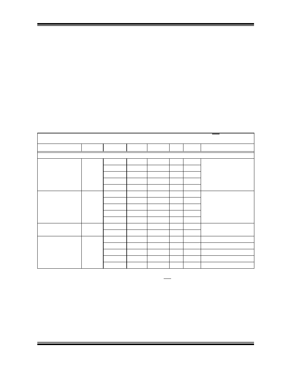
TABLE 1-1:
DC ELECTRICAL SPECIFICATIONS
Electrical Characteristics: Unless otherwise indicated, TA =+25°C, VDD = 1.8V to 5.5V, VSS = GND, EN/CAL =VDD,
VCM =VDD/2, VDM =0V, VREF =VDD/2, VL =VDD/2, RL =10 kΩ to VL and GDM =GMIN; see Figure 1-6 and Figure 1-7.
Parameters
Sym
Min
Typ
Max
Units
GMIN
Conditions
Input Offset
Input Offset Voltage,
Calibrated
VOS
-3.0
—
+3.0
mV
1
-2.0
—
+2.0
mV
2
-0.85
—
+0.85
mV
5
-0.50
—
+0.50
mV
10
-0.35
—
+0.35
mV
100
Input Offset Voltage
Trim Step
VOSTRM
—0.36
—
mV
1
—0.21
—
mV
2
—0.077
—
mV
5
—0.045
—
mV
10
—0.014
—
mV
100
Input Offset Voltage
Drift
ΔVOS/ΔTA
—±90/GMIN
—
V/°C 1 to 10 TA= -40°C to +125°C
—
±2.7
—
V/°C
100
Power Supply
Rejection Ratio
PSRR
62
82
—
dB
1
68
88
—
dB
2
75
96
—
dB
5
81
102
—
dB
10
86
112
—
dB
100
Note 1:
VCM = (VIP + VIM) / 2, VDM = (VIP – VIM) and GDM = 1 + RF/RG.
2:
The VOS spec limits include 1/f noise effects.
3:
This is the input offset drift without VOS re-calibration; toggle EN/CAL to minimize this effect.
4:
These specs apply to both the VIP, VIM input pair (use VCM) and to the VREF, VFG input pair (VREF takes VCM’s place).
5:
This spec applies to the VIP, VIM, VREF and VFG pins individually.
6:
7:
相关PDF资料 |
PDF描述 |
|---|---|
| MCP6V11T-E/OT | IC OPAMP SGL ZERO DRIFT SOT23-5 |
| MCP6V27T-E/SN | IC OPAMP DUAL AUTO-ZERO 8SOIC |
| MCP6V31UT-E/LT | IC OPAMP SGL ZERO DRIFT SC70-5 |
| ME50101VX-000U-A99 | FAN BRUSHLESS 12VDC 50X50X10MM |
| MIC6211BM5 TR | IC OP AMP GEN PURPOSE SOT23-5 |
相关代理商/技术参数 |
参数描述 |
|---|---|
| MCP6S21-I/MS | 功能描述:特殊用途放大器 1-Chan. 12 MHz SPI RoHS:否 制造商:Texas Instruments 通道数量:Single 共模抑制比(最小值): 输入补偿电压: 工作电源电压:3 V to 5.5 V 电源电流:5 mA 最大功率耗散: 最大工作温度:+ 70 C 最小工作温度:- 40 C 安装风格:SMD/SMT 封装 / 箱体:QFN-20 封装:Reel |
| MCP6S21-I/P | 功能描述:特殊用途放大器 1-Chan. 12 MHz SPI RoHS:否 制造商:Texas Instruments 通道数量:Single 共模抑制比(最小值): 输入补偿电压: 工作电源电压:3 V to 5.5 V 电源电流:5 mA 最大功率耗散: 最大工作温度:+ 70 C 最小工作温度:- 40 C 安装风格:SMD/SMT 封装 / 箱体:QFN-20 封装:Reel |
| MCP6S21-I/P | 制造商:Microchip Technology Inc 功能描述:AMP PROGRAMMABLE GAIN 1 CH 6S21 |
| MCP6S21-I/SN | 功能描述:特殊用途放大器 1-Chan. 12 MHz SPI RoHS:否 制造商:Texas Instruments 通道数量:Single 共模抑制比(最小值): 输入补偿电压: 工作电源电压:3 V to 5.5 V 电源电流:5 mA 最大功率耗散: 最大工作温度:+ 70 C 最小工作温度:- 40 C 安装风格:SMD/SMT 封装 / 箱体:QFN-20 封装:Reel |
| MCP6S21-I/SN | 制造商:Microchip Technology Inc 功能描述:Operational Amplifier (Op-Amp) IC |
发布紧急采购,3分钟左右您将得到回复。