- 您现在的位置:买卖IC网 > PDF目录2159 > MCP6N11T-100E/SN (Microchip Technology)IC AMP INSTR RRIO 35MHZ 8SOIC PDF资料下载
参数资料
| 型号: | MCP6N11T-100E/SN |
| 厂商: | Microchip Technology |
| 文件页数: | 22/50页 |
| 文件大小: | 0K |
| 描述: | IC AMP INSTR RRIO 35MHZ 8SOIC |
| 标准包装: | 3,300 |
| 放大器类型: | 仪表 |
| 电路数: | 1 |
| 输出类型: | 满摆幅 |
| 转换速率: | 6 V/µs |
| 增益带宽积: | 35MHz |
| 电流 - 输入偏压: | 10pA |
| 电压 - 输入偏移: | 350µV |
| 电流 - 电源: | 800µA |
| 电流 - 输出 / 通道: | 30mA |
| 电压 - 电源,单路/双路(±): | 1.8 V ~ 5.5 V |
| 工作温度: | -40°C ~ 125°C |
| 安装类型: | 表面贴装 |
| 封装/外壳: | 8-SOIC(0.154",3.90mm 宽) |
| 供应商设备封装: | 8-SOICN |
| 包装: | 带卷 (TR) |
第1页第2页第3页第4页第5页第6页第7页第8页第9页第10页第11页第12页第13页第14页第15页第16页第17页第18页第19页第20页第21页当前第22页第23页第24页第25页第26页第27页第28页第29页第30页第31页第32页第33页第34页第35页第36页第37页第38页第39页第40页第41页第42页第43页第44页第45页第46页第47页第48页第49页第50页
2011 Microchip Technology Inc.
DS25073A-page 29
MCP6N11
4.1.4
AC PERFORMANCE
The bandwidth of these amplifiers depends on GDM
and GMIN:
EQUATION 4-10:
The bandwidth at the maximum output swing is called
the Full Power Bandwidth (fFPBW). It is limited by the
Slew Rate (SR) for many amplifiers, but is close to fBW
for these parts:
EQUATION 4-11:
CMRR is constant from DC to about 1 kHz.
4.1.5
NOISE PERFORMANCE
causes an apparent wander in the DC output voltage.
Changing the measurement time or bandwidth has little
effect on this noise.
We recommend re-calibrating VOS periodically, to
reduce 1/f noise wander. For example, VOS could be
re-calibrated at least once every 15 minutes; more
often when temperature or VDD change significantly.
4.2
Functional Blocks
4.2.1
RAIL-TO-RAIL INPUTS
Each input stage uses one PMOS differential pair at the
input. The output of each differential pair is processed
using current mode circuitry. The inputs show no
crossover distortion vs. common mode voltage.
With this topology, the inputs (VIP and VIM) operate
normally down to VSS – 0.2V and up to VDD + 0.15V at
room temperature (see Figure 2-11). The input offset
voltage (VOS) is measured at VCM =VSS –0.2V and
VDD + 0.15V (at +25°C), to ensure proper operation.
4.2.1.1
Phase Reversal
The input devices are designed to not exhibit phase
inversion when the input pins exceed the supply
exceeding both supplies with no phase inversion.
The input devices also do not exhibit phase inversion
when the differential input voltage exceeds its limits;
4.2.1.2
Input Voltage Limits
In order to prevent damage and/or improper operation
of these amplifiers, the circuit must limit the voltages at
the input pins (see Section 1.1 “Absolute Maximum
Ratings ”). This requirement is independent of the
current limits discussed later on.
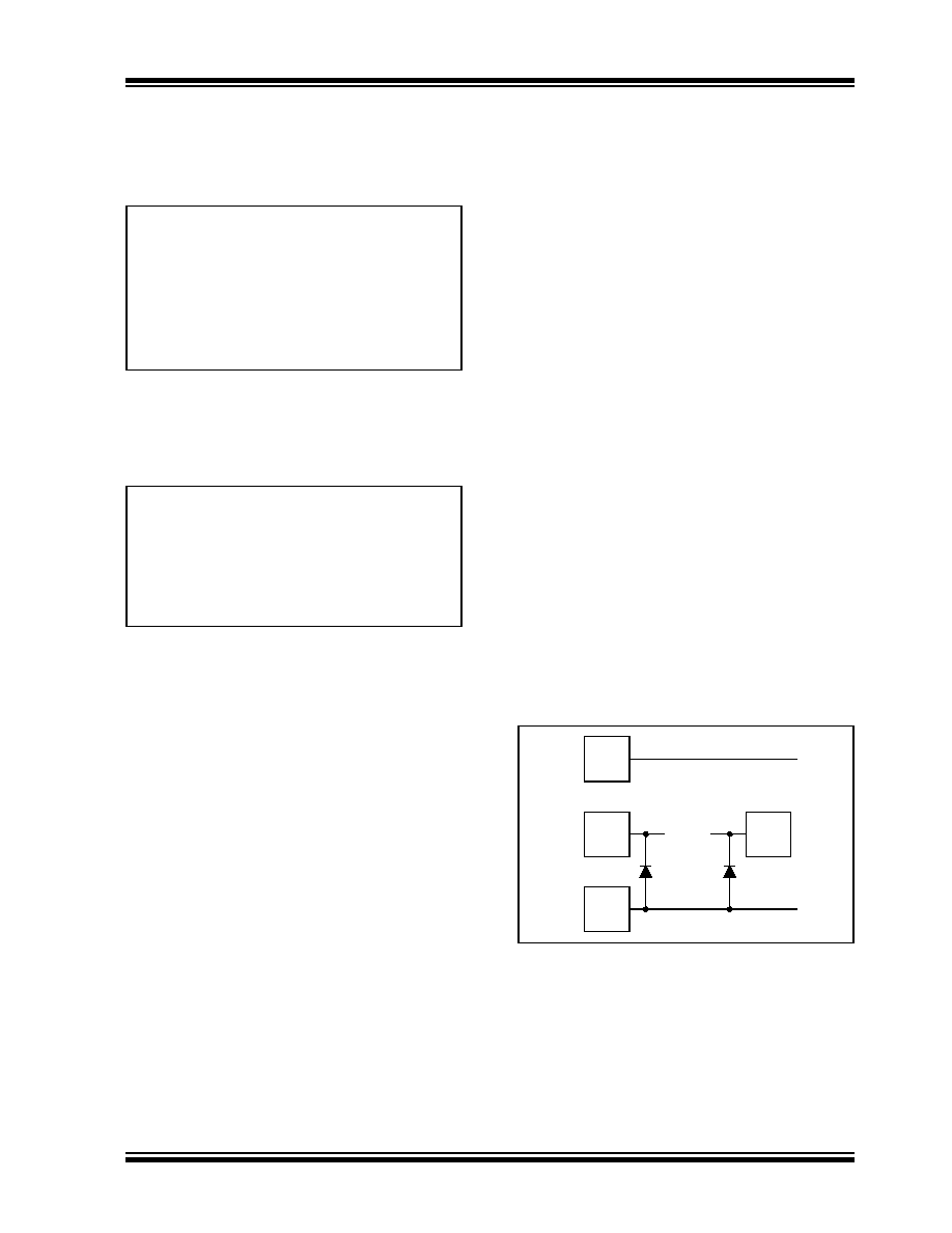
The ESD protection on the inputs can be depicted as
shown in Figure 4-4. This structure was chosen to
protect the input transistors against many (but not all)
overvoltage conditions, and to minimize input bias
current (IB).
FIGURE 4-4:
Simplified Analog Input ESD
Structures.
Where:
fBW = -3 dB bandwidth
fGBWP = Gain bandwidth product
f
BW
f
GBWP
G
DM
---------------
≈
0.50 MHz
() G
MIN GDM
(),
≈
0.35 MHz
() G
MIN GDM
(),
≈
GMIN =1, …, 10
GMIN =100
Where:
V
O = Maximum output voltage swing
≈ VOH –VOL
f
FP BW
SR
πV
O
----------
≈
f
BW
≈
, for these parts
Bond
Pad
Bond
Pad
Bond
Pad
VDD
VIP
VSS
Input
Stage
Bond
Pad
VIM
of
INA Input
相关PDF资料 |
PDF描述 |
|---|---|
| MCP6V11T-E/OT | IC OPAMP SGL ZERO DRIFT SOT23-5 |
| MCP6V27T-E/SN | IC OPAMP DUAL AUTO-ZERO 8SOIC |
| MCP6V31UT-E/LT | IC OPAMP SGL ZERO DRIFT SC70-5 |
| ME50101VX-000U-A99 | FAN BRUSHLESS 12VDC 50X50X10MM |
| MIC6211BM5 TR | IC OP AMP GEN PURPOSE SOT23-5 |
相关代理商/技术参数 |
参数描述 |
|---|---|
| MCP6S21-I/MS | 功能描述:特殊用途放大器 1-Chan. 12 MHz SPI RoHS:否 制造商:Texas Instruments 通道数量:Single 共模抑制比(最小值): 输入补偿电压: 工作电源电压:3 V to 5.5 V 电源电流:5 mA 最大功率耗散: 最大工作温度:+ 70 C 最小工作温度:- 40 C 安装风格:SMD/SMT 封装 / 箱体:QFN-20 封装:Reel |
| MCP6S21-I/P | 功能描述:特殊用途放大器 1-Chan. 12 MHz SPI RoHS:否 制造商:Texas Instruments 通道数量:Single 共模抑制比(最小值): 输入补偿电压: 工作电源电压:3 V to 5.5 V 电源电流:5 mA 最大功率耗散: 最大工作温度:+ 70 C 最小工作温度:- 40 C 安装风格:SMD/SMT 封装 / 箱体:QFN-20 封装:Reel |
| MCP6S21-I/P | 制造商:Microchip Technology Inc 功能描述:AMP PROGRAMMABLE GAIN 1 CH 6S21 |
| MCP6S21-I/SN | 功能描述:特殊用途放大器 1-Chan. 12 MHz SPI RoHS:否 制造商:Texas Instruments 通道数量:Single 共模抑制比(最小值): 输入补偿电压: 工作电源电压:3 V to 5.5 V 电源电流:5 mA 最大功率耗散: 最大工作温度:+ 70 C 最小工作温度:- 40 C 安装风格:SMD/SMT 封装 / 箱体:QFN-20 封装:Reel |
| MCP6S21-I/SN | 制造商:Microchip Technology Inc 功能描述:Operational Amplifier (Op-Amp) IC |
发布紧急采购,3分钟左右您将得到回复。