- 您现在的位置:买卖IC网 > PDF目录2159 > MCP6N11T-100E/SN (Microchip Technology)IC AMP INSTR RRIO 35MHZ 8SOIC PDF资料下载
参数资料
| 型号: | MCP6N11T-100E/SN |
| 厂商: | Microchip Technology |
| 文件页数: | 26/50页 |
| 文件大小: | 0K |
| 描述: | IC AMP INSTR RRIO 35MHZ 8SOIC |
| 标准包装: | 3,300 |
| 放大器类型: | 仪表 |
| 电路数: | 1 |
| 输出类型: | 满摆幅 |
| 转换速率: | 6 V/µs |
| 增益带宽积: | 35MHz |
| 电流 - 输入偏压: | 10pA |
| 电压 - 输入偏移: | 350µV |
| 电流 - 电源: | 800µA |
| 电流 - 输出 / 通道: | 30mA |
| 电压 - 电源,单路/双路(±): | 1.8 V ~ 5.5 V |
| 工作温度: | -40°C ~ 125°C |
| 安装类型: | 表面贴装 |
| 封装/外壳: | 8-SOIC(0.154",3.90mm 宽) |
| 供应商设备封装: | 8-SOICN |
| 包装: | 带卷 (TR) |
第1页第2页第3页第4页第5页第6页第7页第8页第9页第10页第11页第12页第13页第14页第15页第16页第17页第18页第19页第20页第21页第22页第23页第24页第25页当前第26页第27页第28页第29页第30页第31页第32页第33页第34页第35页第36页第37页第38页第39页第40页第41页第42页第43页第44页第45页第46页第47页第48页第49页第50页
MCP6N11
DS25073A-page 32
2011 Microchip Technology Inc.
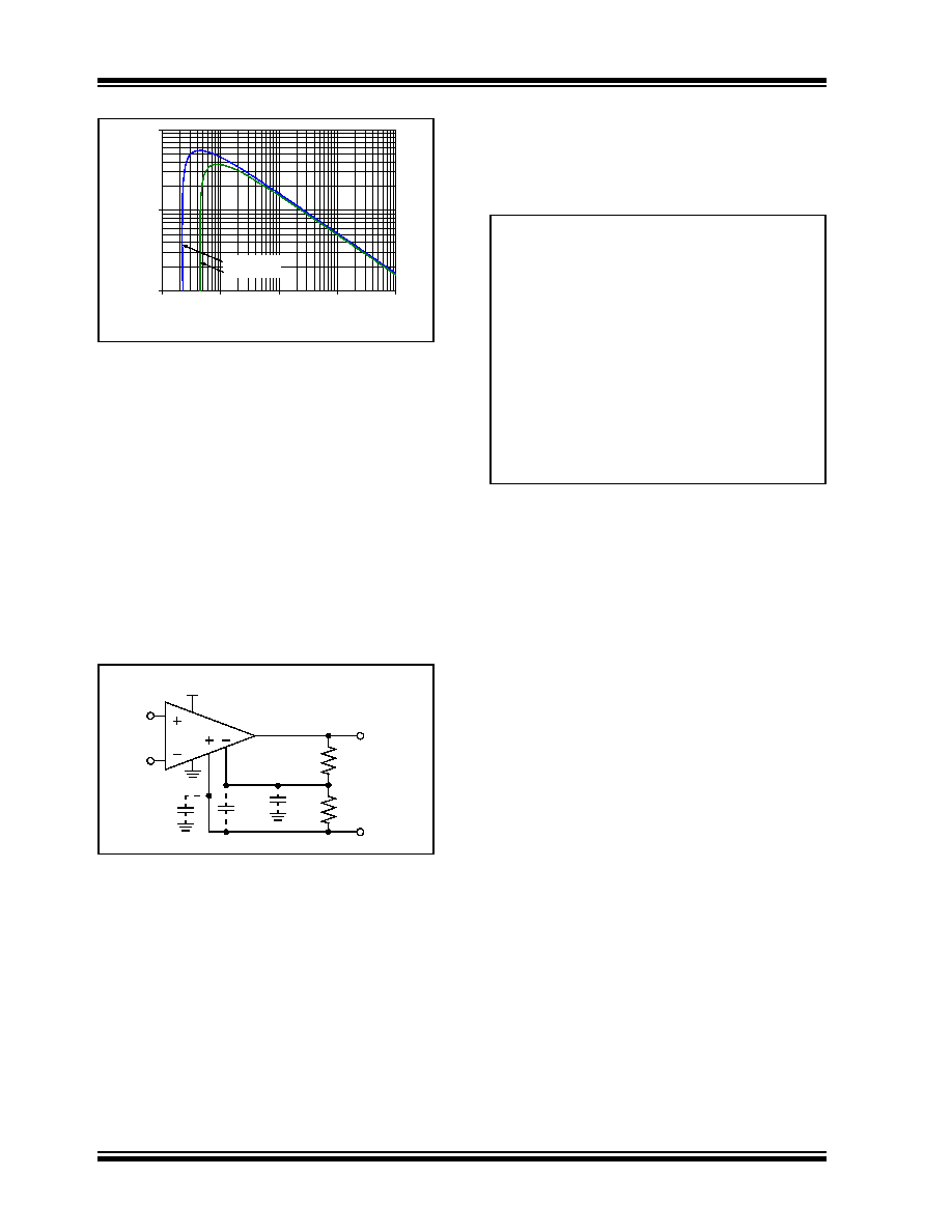
FIGURE 4-9:
Recommended RISO Values
for Capacitive Loads.
After selecting RISO for your circuit, double check the
resulting frequency response peaking and step
response overshoot on the bench. Modify RISO’s value
until the response is reasonable.
4.3.3
GAIN RESISTORS
Figure 4-10 shows a simple gain circuit with the INA’s
input capacitances at the feedback inputs (VREF and
VFG). These capacitances interact with RG and RF to
modify the gain at high frequencies. The equivalent
capacitance acting in parallel to RG is CG =CDM +CCM
plus any board capacitance in parallel to RG. CG will
cause an increase in GDM at high frequencies, which
reduces the phase margin of the feedback loop (i.e.,
reduce the feedback loop's stability).
FIGURE 4-10:
Simple Gain Circuit with
Parasitic Capacitances.
In this data sheet, RF +RG =10 kΩ for most gains (0Ω
Phase Margin. In general, RF (Figure 4-10) needs to
meet the following limits to maintain stability:
EQUATION 4-12:
4.3.4
SUPPLY BYPASS
With these INAs, the power supply pin (VDD for single
supply) should have a local bypass capacitor (i.e.,
0.01 F to 0.1 F) within 2 mm for good high frequency
performance. Surface mount, multilayer ceramic
capacitors, or their equivalent, should be used.
These INAs require a bulk capacitor (i.e., 1.0 F or
larger) within 100 mm, to provide large, slow currents.
This bulk capacitor can be shared with other nearby
analog parts as long as crosstalk through the supplies
does not prove to be a problem.
1.E+03
1.E+04
o
mmended
R
ISO
()
10k
1k
1.E+02
1.E-10
1.E-09
1.E-08
1.E-07
1.E-06
Rec
o
Normalized Load Capacitance;
C
L GMIN/GDM (F)
100
100p
1n
10n
100n
1μ
G
MIN = 1 to 10
G
MIN = 100
VOUT
V1
VDD
V2
VREF
VFG
RF
RG
CDM
CCM
U1
MCP6N11
Where:
α≤ 0.25
GDM ≥ GMIN
fGBWP = Gain Bandwidth Product
CG = CDM + CCM + (PCB stray capacitance)
R
F
0
=
For G
DM =1:
R
F
αG
DM
2
πf
GBWPCG
------------------------------
<
For G
DM >1:
相关PDF资料 |
PDF描述 |
|---|---|
| MCP6V11T-E/OT | IC OPAMP SGL ZERO DRIFT SOT23-5 |
| MCP6V27T-E/SN | IC OPAMP DUAL AUTO-ZERO 8SOIC |
| MCP6V31UT-E/LT | IC OPAMP SGL ZERO DRIFT SC70-5 |
| ME50101VX-000U-A99 | FAN BRUSHLESS 12VDC 50X50X10MM |
| MIC6211BM5 TR | IC OP AMP GEN PURPOSE SOT23-5 |
相关代理商/技术参数 |
参数描述 |
|---|---|
| MCP6S21-I/MS | 功能描述:特殊用途放大器 1-Chan. 12 MHz SPI RoHS:否 制造商:Texas Instruments 通道数量:Single 共模抑制比(最小值): 输入补偿电压: 工作电源电压:3 V to 5.5 V 电源电流:5 mA 最大功率耗散: 最大工作温度:+ 70 C 最小工作温度:- 40 C 安装风格:SMD/SMT 封装 / 箱体:QFN-20 封装:Reel |
| MCP6S21-I/P | 功能描述:特殊用途放大器 1-Chan. 12 MHz SPI RoHS:否 制造商:Texas Instruments 通道数量:Single 共模抑制比(最小值): 输入补偿电压: 工作电源电压:3 V to 5.5 V 电源电流:5 mA 最大功率耗散: 最大工作温度:+ 70 C 最小工作温度:- 40 C 安装风格:SMD/SMT 封装 / 箱体:QFN-20 封装:Reel |
| MCP6S21-I/P | 制造商:Microchip Technology Inc 功能描述:AMP PROGRAMMABLE GAIN 1 CH 6S21 |
| MCP6S21-I/SN | 功能描述:特殊用途放大器 1-Chan. 12 MHz SPI RoHS:否 制造商:Texas Instruments 通道数量:Single 共模抑制比(最小值): 输入补偿电压: 工作电源电压:3 V to 5.5 V 电源电流:5 mA 最大功率耗散: 最大工作温度:+ 70 C 最小工作温度:- 40 C 安装风格:SMD/SMT 封装 / 箱体:QFN-20 封装:Reel |
| MCP6S21-I/SN | 制造商:Microchip Technology Inc 功能描述:Operational Amplifier (Op-Amp) IC |
发布紧急采购,3分钟左右您将得到回复。