- 您现在的位置:买卖IC网 > PDF目录2159 > MCP6N11T-100E/SN (Microchip Technology)IC AMP INSTR RRIO 35MHZ 8SOIC PDF资料下载
参数资料
| 型号: | MCP6N11T-100E/SN |
| 厂商: | Microchip Technology |
| 文件页数: | 25/50页 |
| 文件大小: | 0K |
| 描述: | IC AMP INSTR RRIO 35MHZ 8SOIC |
| 标准包装: | 3,300 |
| 放大器类型: | 仪表 |
| 电路数: | 1 |
| 输出类型: | 满摆幅 |
| 转换速率: | 6 V/µs |
| 增益带宽积: | 35MHz |
| 电流 - 输入偏压: | 10pA |
| 电压 - 输入偏移: | 350µV |
| 电流 - 电源: | 800µA |
| 电流 - 输出 / 通道: | 30mA |
| 电压 - 电源,单路/双路(±): | 1.8 V ~ 5.5 V |
| 工作温度: | -40°C ~ 125°C |
| 安装类型: | 表面贴装 |
| 封装/外壳: | 8-SOIC(0.154",3.90mm 宽) |
| 供应商设备封装: | 8-SOICN |
| 包装: | 带卷 (TR) |
第1页第2页第3页第4页第5页第6页第7页第8页第9页第10页第11页第12页第13页第14页第15页第16页第17页第18页第19页第20页第21页第22页第23页第24页当前第25页第26页第27页第28页第29页第30页第31页第32页第33页第34页第35页第36页第37页第38页第39页第40页第41页第42页第43页第44页第45页第46页第47页第48页第49页第50页
2011 Microchip Technology Inc.
DS25073A-page 31
MCP6N11
4.2.2
ENABLE/VOS CALIBRATION
(EN/CAL)
These parts have a Normal mode, a Low Power mode
and a VOS Calibration mode.
When the EN/CAL pin is high and the internal POR
(with delay) indicates that power is good, the part
operates in its Normal mode.
When the EN/CAL pin is low, the part operates in its
Low Power mode. The quiescent current (at VSS) drops
to -2.5 A (typical), the amplifier output is put into a
high-impedance state. Signals at the input pins can
feed through to the output pin.
When the EN/CAL pin goes high and the internal POR
(with delay) indicates that power is good, the amplifier
internally corrects its input offset voltage (VOS) with the
internal common mode voltage at mid-supply (VDD/2)
and the output tri-stated (after tOFF). Once VOS Calibra-
tion is completed, the amplifier is enabled and normal
operation resumes.
The EN/CAL pin does not operate normally when left
floating. Either drive it with a logic output, or tie it high
so that the part is always on.
4.2.3
POR WITH DELAY
The internal POR makes sure that the input offset
voltage (VOS) is calibrated whenever the supply
voltage goes from low voltage (< VPRL) to high voltage
(> VPRH). This prevents corruption of the VOS trim reg-
isters after a low-power event.
After the POR goes high, the internal circuitry adds a
fixed delay (tPLH), before telling the VOS Calibration
circuitry (see Figure 4-2) to start. If the EN/CAL pin is
toggled during this time, the fixed delay is restarted
(takes an additional time tPLH).
4.2.4
PARITY DETECTOR
A parity error detector monitors the memory contents
for any corruption. In the rare event that a parity error is
detected (e.g., corruption from an alpha particle), a
POR event is automatically triggered. This will cause
the input offset voltage to be re-corrected, and the op
amp will not return to normal operation for a period of
time (the POR turn on time, tPLH).
4.2.5
RAIL-TO-RAIL OUTPUT
The Minimum Output Voltage (VOL) and Maximum
Output Voltage (VOH) specs describe the widest output
swing that can be achieved under the specified load
conditions.
The output can also be limited when VIP or VIM exceeds
VIVL or VIVH, or when VDM exceeds VDML or VDMH.
4.3
Applications Tips
4.3.1
MINIMUM STABLE GAIN
There are different options for different Minimum Stable
Gains (1, 2, 5, 10 and 100 V/V; see Table 1-1). The
differential gain (GDM) needs to be greater than or
equal to GMIN in order to maintain stability.
Picking a part with higher GMIN has the advantages of
lower Input Noise Voltage Density (eni), lower Input
Offset Voltage (VOS) and increased Gain Bandwidth
Product (GBWP); see Table 1. The Differential Input
Voltage Range (VDMR) is lower for higher GMIN, but the
output voltage range would limit VDMR anyway, when
GDM ≥ 2.
4.3.2
CAPACITIVE LOADS
Driving large capacitive loads can cause stability
problems for amplifiers. As the load capacitance
increases,
the
feedback
loop’s
phase
margin
decreases, and the closed-loop bandwidth is reduced.
This produces gain peaking in the frequency response,
with overshoot and ringing in the step response. Lower
gains (GDM) exhibit greater sensitivity to capacitive
loads.
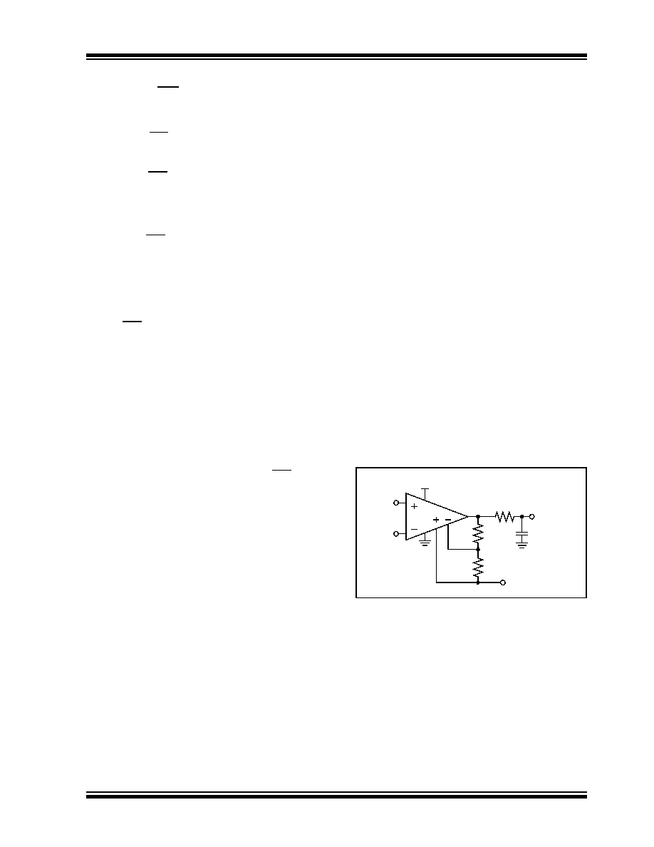
When driving large capacitive loads with these
instrumentation amps (e.g., > 100 pF), a small series
feedback loop’s phase margin (stability) by making the
output load resistive at higher frequencies. The
bandwidth will be generally lower than the bandwidth
with no capacitive load.
FIGURE 4-8:
Output Resistor, RISO
stabilizes large capacitive loads.
different capacitive loads and gains. The x-axis is the
normalized load capacitance (CL GMIN/GDM), where
GDM is the circuit’s differential gain (1 + RF /RG) and
GMIN is the minimum stable gain.
RISO
VOUT
CL
V1
VDD
V2
VREF
VFG
RF
RG
U1
MCP6N11
相关PDF资料 |
PDF描述 |
|---|---|
| MCP6V11T-E/OT | IC OPAMP SGL ZERO DRIFT SOT23-5 |
| MCP6V27T-E/SN | IC OPAMP DUAL AUTO-ZERO 8SOIC |
| MCP6V31UT-E/LT | IC OPAMP SGL ZERO DRIFT SC70-5 |
| ME50101VX-000U-A99 | FAN BRUSHLESS 12VDC 50X50X10MM |
| MIC6211BM5 TR | IC OP AMP GEN PURPOSE SOT23-5 |
相关代理商/技术参数 |
参数描述 |
|---|---|
| MCP6S21-I/MS | 功能描述:特殊用途放大器 1-Chan. 12 MHz SPI RoHS:否 制造商:Texas Instruments 通道数量:Single 共模抑制比(最小值): 输入补偿电压: 工作电源电压:3 V to 5.5 V 电源电流:5 mA 最大功率耗散: 最大工作温度:+ 70 C 最小工作温度:- 40 C 安装风格:SMD/SMT 封装 / 箱体:QFN-20 封装:Reel |
| MCP6S21-I/P | 功能描述:特殊用途放大器 1-Chan. 12 MHz SPI RoHS:否 制造商:Texas Instruments 通道数量:Single 共模抑制比(最小值): 输入补偿电压: 工作电源电压:3 V to 5.5 V 电源电流:5 mA 最大功率耗散: 最大工作温度:+ 70 C 最小工作温度:- 40 C 安装风格:SMD/SMT 封装 / 箱体:QFN-20 封装:Reel |
| MCP6S21-I/P | 制造商:Microchip Technology Inc 功能描述:AMP PROGRAMMABLE GAIN 1 CH 6S21 |
| MCP6S21-I/SN | 功能描述:特殊用途放大器 1-Chan. 12 MHz SPI RoHS:否 制造商:Texas Instruments 通道数量:Single 共模抑制比(最小值): 输入补偿电压: 工作电源电压:3 V to 5.5 V 电源电流:5 mA 最大功率耗散: 最大工作温度:+ 70 C 最小工作温度:- 40 C 安装风格:SMD/SMT 封装 / 箱体:QFN-20 封装:Reel |
| MCP6S21-I/SN | 制造商:Microchip Technology Inc 功能描述:Operational Amplifier (Op-Amp) IC |
发布紧急采购,3分钟左右您将得到回复。