- 您现在的位置:买卖IC网 > PDF目录385639 > MT28F320A18 (Micron Technology, Inc.) FLASH MEMORY PDF资料下载
参数资料
| 型号: | MT28F320A18 |
| 厂商: | Micron Technology, Inc. |
| 英文描述: | FLASH MEMORY |
| 中文描述: | 闪存 |
| 文件页数: | 10/37页 |
| 文件大小: | 558K |
| 代理商: | MT28F320A18 |
第1页第2页第3页第4页第5页第6页第7页第8页第9页当前第10页第11页第12页第13页第14页第15页第16页第17页第18页第19页第20页第21页第22页第23页第24页第25页第26页第27页第28页第29页第30页第31页第32页第33页第34页第35页第36页第37页
2 MEG x 16
1.8V ENHANCED+ BOOT BLOCK FLASH MEMORY
PRELIMINARY
2 Meg x 16, 1.8V Enhanced+ Boot Block Flash Memory
MT28F320A18_3.fm - Rev. 3, Pub. 9/2002
2002, Micron Technology Inc.
10
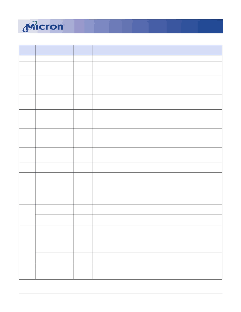
Table 5:
Command Descriptions
CODE
10h
20h
DEVICE MODE
Alt. Program Setup
BUS
CYCLE
First
First
DESCRIPTION
Operates the same as a PROGRAM SETUP command.
Erase Setup
Prepares the CSM for an ERASE CONFIRM command. If the next command is
not an ERASE CONFIRM command, the command will be ignored, and the
device will go to read status mode and wait for another command.
40h
Program Setup
First
A two-cycle command: The first cycle prepares for a PROGRAM operation, the
second cycle latches addresses and data and initiates the WSM to execute the
program algorithm. The Flash device outputs status register data on the
falling edge of OE# or CE#, whichever occurs first.
50h
Clear Status Register
First
The WSM can set the block lock status (SR1), V
PP
Status (SR3), program status
(SR4),and erase status (SR5) bits in the status register to “1,” but it cannot
clear them to “0.” Issuing this command clears those bits to “0.”
60h
Protection
Configuration Setup
First
Prepares the CSM for changes to the block locking status. If the next
command is not BLOCK UNLOCK, BLOCK LOCK, or BLOCK LOCK DOWN, then
the CSM will set both the program and erase status register bits to indicate a
command sequence error.
Places the device into read status register mode. Reading the device will
output the contents of the status register for the addressed bank. The device
will automatically enter this mode for the addressed bank after a PROGRAM
or ERASE operation has been initiated.
70h
Read Status Register
First
90h
Read Protection
Configuration
Register
First
Puts the device into the read protection configuration register mode so that
reading the device will output the manufacturer/device codes, block lock
status, protection register, or protection register lock.
98h
Read Query
First
Puts the device into the read query mode so that reading the device will
output common flash interface information.
Suspends the currently executing PROGRAM/ERASE operation. The status
register will indicate when the operation has been successfully suspended by
setting either the program suspend (SR2) or erase suspend (SR6) and the
WSM status bit (SR7) to a “1” (ready). The WSM will continue to idle in the
suspend state, regardless of the state of all input control pins except RP#,
which will immediately shut down the WSM and the remainder of the chip if
RP# is driven to V
IL
.
B0h
Program/Erase
Suspend
First
C0h
Program Device
Protection Register
Lock Device
Protection Register
First
Writes a specific code into the device protection register.
First
Locks the device protection register; data can no longer be changed.
D0h
Erase Confirm
Second
If the previous command was an ERASE SETUP command, then the CSM will
close the address and data latches, and it will begin erasing the block
indicated on the address pins. During programming/erase, the device will
respond only to the READ STATUS REGISTER, PROGRAM/ERASE SUSPEND
commands and will output status register data on the falling edge of OE# or
CE#, whichever occurs last.
Program/Erase
Resume
First
If a program or erase operation was previously suspended, this command will
resume the operation.
FFh
Read Array
First
During the read array mode, array data will be output on the data bus.
01h
Lock Block
Second
If the previous command was PROTECTION CONFIGURATION SETUP, the CSM
will latch the address and lock the block indicated on the address bus.
相关PDF资料 |
PDF描述 |
|---|---|
| MT2D18 | 1 Meg x 8 DRAM Module(5V,1M x 8 动态RAM模块) |
| MT46V16M4 | 4 Meg x 4 x 4 banks DDR SDRAM(4 M x 4 x 4组,双数据速率同步动态RAM) |
| MT46V4M16 | 1 Meg x 16 x 4 banks DDR SDRAM(1M x 16 x 4组,双数据速率同步动态RAM) |
| MT46V8M8 | 2 Meg x 8 x 4 banks DDR SDRAM(2 M x 8 x 4组,双数据速率同步动态RAM) |
| MT46V2M32LG | DOUBLE DATA RATE DDR SDRAM |
相关代理商/技术参数 |
参数描述 |
|---|---|
| MT28F320J3 | 制造商:MICRON 制造商全称:Micron Technology 功能描述:Q-FLASHTM MEMORY |
| MT28F320J3BS-11 ET | 功能描述:IC FLASH 32MBIT 110NS 64FBGA RoHS:是 类别:集成电路 (IC) >> 存储器 系列:- 标准包装:1 系列:- 格式 - 存储器:RAM 存储器类型:SDRAM 存储容量:256M(8Mx32) 速度:143MHz 接口:并联 电源电压:3 V ~ 3.6 V 工作温度:-40°C ~ 85°C 封装/外壳:90-VFBGA 供应商设备封装:90-VFBGA(8x13) 包装:托盘 其它名称:Q2841869 |
| MT28F320J3BS-11 ET TR | 功能描述:IC FLASH 32MBIT 110NS 64FBGA RoHS:是 类别:集成电路 (IC) >> 存储器 系列:- 标准包装:378 系列:- 格式 - 存储器:闪存 存储器类型:FLASH 存储容量:8M(1M x 8,512K x 16) 速度:110ns 接口:并联 电源电压:2.7 V ~ 3.6 V 工作温度:-40°C ~ 85°C 封装/外壳:48-CBGA 供应商设备封装:48-CBGA(7x7) 包装:托盘 |
| MT28F320J3BS-11 GMET | 功能描述:IC FLASH 32MBIT 110NS 64FBGA RoHS:是 类别:集成电路 (IC) >> 存储器 系列:- 标准包装:1 系列:- 格式 - 存储器:RAM 存储器类型:SDRAM 存储容量:256M(8Mx32) 速度:143MHz 接口:并联 电源电压:3 V ~ 3.6 V 工作温度:-40°C ~ 85°C 封装/外壳:90-VFBGA 供应商设备封装:90-VFBGA(8x13) 包装:托盘 其它名称:Q2841869 |
| MT28F320J3BS-11 GMET TR | 功能描述:IC FLASH 32MBIT 110NS 64FBGA RoHS:是 类别:集成电路 (IC) >> 存储器 系列:- 标准包装:378 系列:- 格式 - 存储器:闪存 存储器类型:FLASH 存储容量:8M(1M x 8,512K x 16) 速度:110ns 接口:并联 电源电压:2.7 V ~ 3.6 V 工作温度:-40°C ~ 85°C 封装/外壳:48-CBGA 供应商设备封装:48-CBGA(7x7) 包装:托盘 |
发布紧急采购,3分钟左右您将得到回复。