- 您现在的位置:买卖IC网 > Datasheet目录345 > MT48H8M16LFB4-75 IT:K TR (Micron Technology Inc)IC SDRAM 128MBIT 133MHZ 54VFBGA Datasheet资料下载
参数资料
| 型号: | MT48H8M16LFB4-75 IT:K TR |
| 厂商: | Micron Technology Inc |
| 文件页数: | 10/63页 |
| 文件大小: | 0K |
| 描述: | IC SDRAM 128MBIT 133MHZ 54VFBGA |
| 标准包装: | 1 |
| 格式 - 存储器: | RAM |
| 存储器类型: | 移动 SDRAM |
| 存储容量: | 128M(8Mx16) |
| 速度: | 133MHz |
| 接口: | 并联 |
| 电源电压: | 1.7 V ~ 1.95 V |
| 工作温度: | -40°C ~ 85°C |
| 封装/外壳: | 54-VFBGA |
| 供应商设备封装: | 54-VFBGA(8x8) |
| 包装: | 标准包装 |
| 其它名称: | 557-1530-6 |
第1页第2页第3页第4页第5页第6页第7页第8页第9页当前第10页第11页第12页第13页第14页第15页第16页第17页第18页第19页第20页第21页第22页第23页第24页第25页第26页第27页第28页第29页第30页第31页第32页第33页第34页第35页第36页第37页第38页第39页第40页第41页第42页第43页第44页第45页第46页第47页第48页第49页第50页第51页第52页第53页第54页第55页第56页第57页第58页第59页第60页第61页第62页第63页
�� �
�
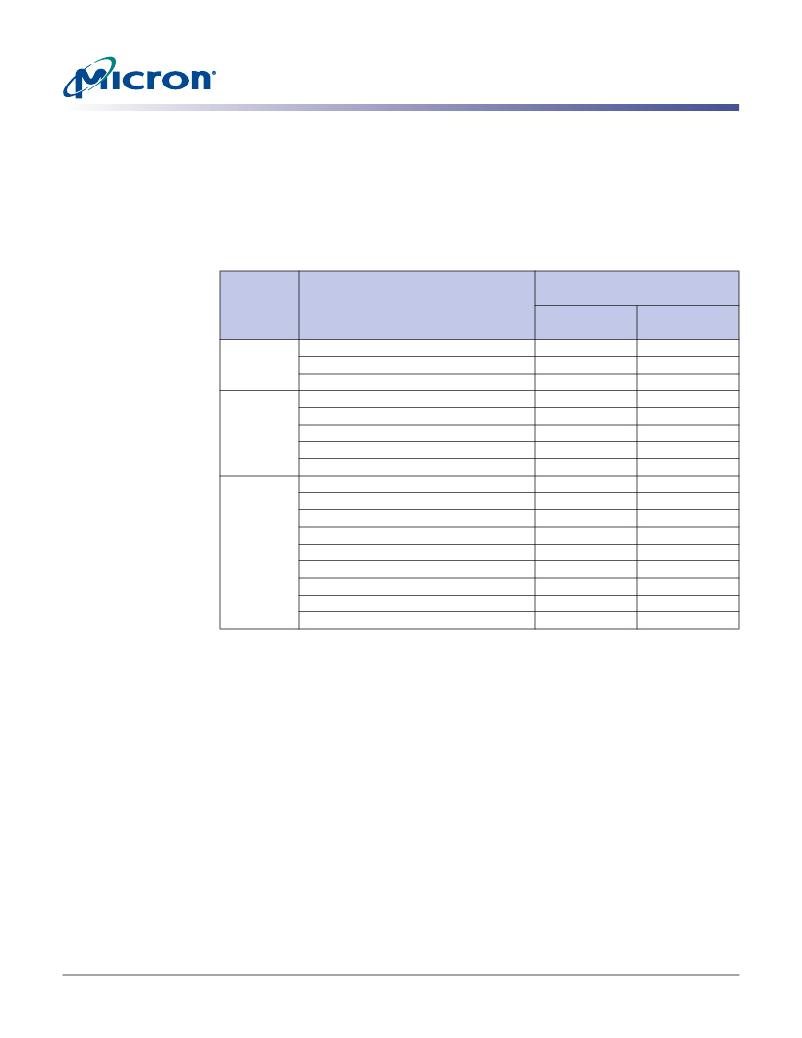
�128Mb:� x16� Mobile� SDRAM�
�Mode� Register� Definition�
�Burst� Type�
�Accesses� within� a� given� burst� may� be� programmed� to� be� either� sequential� or� interleaved;�
�this� is� referred� to� as� the� burst� type� and� is� selected� via� bit� M3.�
�The� ordering� of� accesses� within� a� burst� is� determined� by� BL,� the� burst� type,� and� the�
�starting� column� address,� as� shown� in� Table� 4� on� page� 10.�
�Table� 4:�
�Burst� Definition�
�Note� 1�
�Order� of� Accesses� Within� a�
�Burst�
�Burst�
�Type� =�
�Type� =�
�Length�
�2� 2�
�4� 3�
�Starting� Column� Address�
�A0�
�0�
�1�
�A1�
�A0�
�Sequential�
�0-1�
�1-0�
�Interleaved�
�0-1�
�1-0�
�0�
�0�
�1�
�1�
�0�
�1�
�0�
�1�
�0-1-2-3�
�1-2-3-0�
�2-3-0-1�
�3-0-1-2�
�0-1-2-3�
�1-0-3-2�
�2-3-0-1�
�3-2-1-0�
�8� 4�
�A2�
�A1�
�A0�
�0�
�0�
�0�
�0�
�1�
�1�
�1�
�1�
�0�
�0�
�1�
�1�
�0�
�0�
�1�
�1�
�0�
�1�
�0�
�1�
�0�
�1�
�0�
�1�
�0-1-2-3-4-5-6-7�
�1-2-3-4-5-6-7-0�
�2-3-4-5-6-7-0-1�
�3-4-5-6-7-0-1-2�
�4-5-6-7-0-1-2-3�
�5-6-7-0-1-2-3-4�
�6-7-0-1-2-3-4-5�
�7-0-1-2-3-4-5-6�
�0-1-2-3-4-5-6-7�
�1-0-3-2-5-4-7-6�
�2-3-0-1-6-7-4-5�
�3-2-1-0-7-6-5-4�
�4-5-6-7-0-1-2-3�
�5-4-7-6-1-0-3-2�
�6-7-4-5-2-3-0-1�
�7-6-5-4-3-2-1-0�
�Notes:�
�1.� Whenever� a� boundary� of� the� block� is� reached� within� a� given� sequence� above,� the� following�
�access� wraps� within� the� block.�
�2.� For� BL� =� 2,� A1–A8� select� the� block-of-two� burst;� A0� selects� the� starting� column� within� the�
�block.�
�3.� For� BL� =� 4,� A2–A8� select� the� block-of-four� burst;� A0–A1� select� the� starting� column� within�
�the� block.�
�4.� For� BL� =� 8,� A3–A8� select� the� block-of-eight� burst;� A0–A2� select� the� starting� column� within�
�the� block.�
�CAS� Latency� (CL)�
�The� CL� is� the� delay,� in� clock� cycles,� between� the� registration� of� a� READ� command� and�
�the� availability� of� the� first� piece� of� output� data.� The� latency� can� be� set� to� two� or� three�
�clocks.�
�If� a� READ� command� is� registered� at� clock� edge� n� ,� and� the� latency� is� m� clocks,� the� data�
�will� be� available� by� clock� edge� n� +� m� .� The� DQs� will� start� driving� as� a� result� of� the� clock�
�edge� one� cycle� earlier� (� n� +� m� -� 1),� and� provided� that� the� relevant� access� times� are� met,�
�the� data� will� be� valid� by� clock� edge� n� +� m� .� For� example,� assuming� that� the� clock� cycle�
�time� is� such� that� all� relevant� access� times� are� met,� if� a� READ� command� is� registered� at� T0�
�PDF:� 09005aef8237e877/Source:� 09005aef8237e8d8�
�128Mb_x16� Mobile� SDRAM_Y25M_2.fm� -� Rev.� C� 2/07� EN�
�10�
�Micron� Technology,� Inc.,� reserves� the� right� to� change� products� or� specifications� without� notice.�
�?2006� Micron� Technology,� Inc.� All� rights� reserved.�
�相关PDF资料 |
PDF描述 |
|---|---|
| MTC100-JA2-P34 | CONTACT INSERT PIN |
| MX841BE | IC CONVERTER WHITE LED 8-SOIC |
| MXHV9910BTR | IC LED DRIVER HIGH BRIGHT 8-SOIC |
| MXN12FB12F | MOTOR BRUSHED DC 12V 2922RPM |
| MXN13FB08B1 | MOTOR BRUSHED DC 8V 4714RPM |
相关代理商/技术参数 |
参数描述 |
|---|---|
| MT48H8M16LFB4-8 | 制造商:Micron Technology Inc 功能描述:IC SDRAM 128MBIT 125MHZ 54VFBGA |
| MT48H8M16LFB4-8 IT | 制造商:Micron Technology Inc 功能描述:IC SDRAM 128MBIT 125MHZ 54VFBGA |
| MT48H8M16LFB4-8 IT TR | 功能描述:IC SDRAM 128MBIT 125MHZ 54VFBGA RoHS:是 类别:集成电路 (IC) >> 存储器 系列:- 标准包装:96 系列:- 格式 - 存储器:闪存 存储器类型:FLASH 存储容量:16M(2M x 8,1M x 16) 速度:70ns 接口:并联 电源电压:2.65 V ~ 3.6 V 工作温度:-40°C ~ 85°C 封装/外壳:48-TFSOP(0.724",18.40mm 宽) 供应商设备封装:48-TSOP 包装:托盘 |
发布紧急采购,3分钟左右您将得到回复。