- 您现在的位置:买卖IC网 > Datasheet目录345 > MT48H8M16LFB4-75 IT:K TR (Micron Technology Inc)IC SDRAM 128MBIT 133MHZ 54VFBGA Datasheet资料下载
参数资料
| 型号: | MT48H8M16LFB4-75 IT:K TR |
| 厂商: | Micron Technology Inc |
| 文件页数: | 7/63页 |
| 文件大小: | 0K |
| 描述: | IC SDRAM 128MBIT 133MHZ 54VFBGA |
| 标准包装: | 1 |
| 格式 - 存储器: | RAM |
| 存储器类型: | 移动 SDRAM |
| 存储容量: | 128M(8Mx16) |
| 速度: | 133MHz |
| 接口: | 并联 |
| 电源电压: | 1.7 V ~ 1.95 V |
| 工作温度: | -40°C ~ 85°C |
| 封装/外壳: | 54-VFBGA |
| 供应商设备封装: | 54-VFBGA(8x8) |
| 包装: | 标准包装 |
| 其它名称: | 557-1530-6 |
第1页第2页第3页第4页第5页第6页当前第7页第8页第9页第10页第11页第12页第13页第14页第15页第16页第17页第18页第19页第20页第21页第22页第23页第24页第25页第26页第27页第28页第29页第30页第31页第32页第33页第34页第35页第36页第37页第38页第39页第40页第41页第42页第43页第44页第45页第46页第47页第48页第49页第50页第51页第52页第53页第54页第55页第56页第57页第58页第59页第60页第61页第62页第63页
�� �
�
�128Mb:� x16� Mobile� SDRAM�
�General� Description�
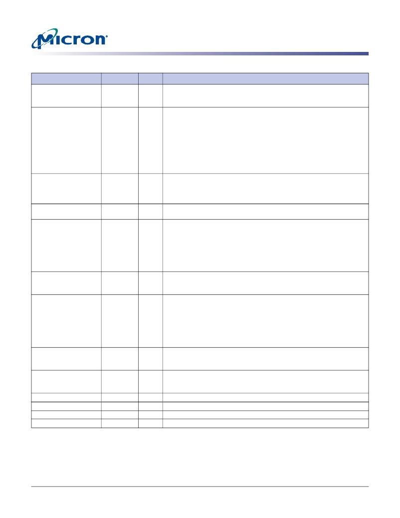
�Table� 3:�
�Ball� Descriptions�
�54-BALL� FBGA�
�F2�
�SYMBOL�
�CLK�
�TYPE�
�Input�
�DESCRIPTION�
�Clock:� CLK� is� driven� by� the� system� clock.� All� SDRAM� input� signals� are�
�sampled� on� the� positive� edge� of� CLK.� CLK� also� increments� the� internal�
�burst� counter� and� controls� the� output� registers.�
�F3�
�CKE�
�Input�
�Clock� enable:� CKE� activates� (HIGH)� and� deactivates� (LOW)� the� CLK� signal.�
�Deactivating� the� clock� provides� PRECHARGE� power-down� and� SELF�
�REFRESH� operation� (all� banks� idle),� ACTIVE� power-down� (row� active� in�
�any� bank),� deep� power-down� (all� banks� idle),� or� CLOCK� SUSPEND�
�operation� (burst/access� in� progress).� CKE� is� synchronous� except� after� the�
�device� enters� power-down� and� self� refresh� modes,� where� CKE� becomes�
�asynchronous� until� after� exiting� the� same� mode.� The� input� buffers,�
�including� CLK,� are� disabled� during� power-down� and� self� refresh� modes,�
�providing� low� standby� power.� CKE� may� be� tied� HIGH.�
�G9�
�CS#�
�Input�
�Chip� select:� CS#� enables� (registered� LOW)� and� disables� (registered� HIGH)�
�the� command� decoder.� All� commands� are� masked� when� CS#� is� registered�
�HIGH.� CS#� provides� for� external� bank� selection� on� systems� with� multiple�
�banks.� CS#� is� considered� part� of� the� command� code.�
�F7,� F8,� F9�
�E8,� F1�
�CAS#,� RAS#,�
�WE#�
�LDQM,�
�UDQM�
�Input�
�Input�
�Command� inputs:� CAS#,� RAS#,� and� WE#� (along� with� CS#)� define� the�
�command� being� entered.�
�Input/Output� mask:� DQM� is� sampled� HIGH� and� is� an� input� mask� signal� for�
�write� accesses� and� an� output� enable� signal� for� read� accesses.� Input� data� is�
�masked� during� a� WRITE� cycle.� The� output� buffers� are� placed� in� a� High-Z�
�state� (two-clock� latency)� during� a� READ� cycle.� LDQM� corresponds� to� DQ0–�
�DQ7,� UDQM� corresponds� to� DQ8–DQ15.� LDQM� and� UDQM� are� considered�
�same� state� when� referenced� as� DQM.� DQM� loading� is� designed� to� match�
�that� of� DQ� balls.�
�G7,� G8�
�BA0,� BA1�
�Input�
�Bank� address� input(s):� BA0� and� BA1� define� to� which� bank� the� ACTIVE,�
�READ,� WRITE,� or� PRECHARGE� command� is� being� applied.� These� balls� also�
�select� between� the� mode� register� and� the� extended� mode� register.�
�H7,� H8,� J8,� J7,� J3,� J2,� H3,�
�H2,� H1,� G3,� H9,� G2�
�A0–A11�
�Input�
�Address� inputs:� Provide� the� row� address� for� ACTIVE� commands,� and� the�
�column� address� and� auto� precharge� bit� (A10)� for� READ� or� WRITE�
�commands,� to� select� one� location� out� of� the� memory� array� in� the�
�respective� bank.� During� a� PRECHARGE� command,� A10� determines�
�whether� the� PRECHARGE� applies� to� one� bank� (A10� LOW,� bank� selected� by�
�BA0,� BA1)� or� all� banks� (A10� HIGH).� The� address� inputs� also� provide� the� op-�
�code� during� a� LOAD� MODE� REGISTER� command.�
�A8,� B9,� B8,� C9,� C8,� D9,�
�DQ0–DQ15�
�I/O�
�Data� input/output:� Data� bus.�
�D8,� E9,� E1,� D2,� D1,� C2,�
�C1,� B2,� B1,� A2�
�E2,� G1�
�DNU/NC�
�–�
�DNU� =� do� not� use:� Must� be� left� unconnected.�
�NC� =� no� connect� (internally� unconnected):� Can� be� left� unconnected,� but� it�
�is� recommended� that� it� is� connected� to� V� SS� .�
�A7,� B3,� C7,� D3�
�A3,� B7,� C3,� D7�
�A9,� E7,� J9�
�A1,� E3,� J1�
�V� DD� Q�
�V� SS� Q�
�V� DD�
�V� SS�
�Supply�
�Supply�
�Supply�
�Supply�
�DQ� power:� Provide� isolated� power� to� DQs� for� improved� noise� immunity.�
�DQ� ground:� Provide� isolated� ground� to� DQs� for� improved� noise� immunity.�
�Core� power� supply.�
�Ground.�
�PDF:� 09005aef8237e877/Source:� 09005aef8237e8d8�
�128Mb_x16� Mobile� SDRAM_Y25M_2.fm� -� Rev.� C� 2/07� EN�
�7�
�Micron� Technology,� Inc.,� reserves� the� right� to� change� products� or� specifications� without� notice.�
�?2006� Micron� Technology,� Inc.� All� rights� reserved.�
�相关PDF资料 |
PDF描述 |
|---|---|
| MTC100-JA2-P34 | CONTACT INSERT PIN |
| MX841BE | IC CONVERTER WHITE LED 8-SOIC |
| MXHV9910BTR | IC LED DRIVER HIGH BRIGHT 8-SOIC |
| MXN12FB12F | MOTOR BRUSHED DC 12V 2922RPM |
| MXN13FB08B1 | MOTOR BRUSHED DC 8V 4714RPM |
相关代理商/技术参数 |
参数描述 |
|---|---|
| MT48H8M16LFB4-8 | 制造商:Micron Technology Inc 功能描述:IC SDRAM 128MBIT 125MHZ 54VFBGA |
| MT48H8M16LFB4-8 IT | 制造商:Micron Technology Inc 功能描述:IC SDRAM 128MBIT 125MHZ 54VFBGA |
| MT48H8M16LFB4-8 IT TR | 功能描述:IC SDRAM 128MBIT 125MHZ 54VFBGA RoHS:是 类别:集成电路 (IC) >> 存储器 系列:- 标准包装:96 系列:- 格式 - 存储器:闪存 存储器类型:FLASH 存储容量:16M(2M x 8,1M x 16) 速度:70ns 接口:并联 电源电压:2.65 V ~ 3.6 V 工作温度:-40°C ~ 85°C 封装/外壳:48-TFSOP(0.724",18.40mm 宽) 供应商设备封装:48-TSOP 包装:托盘 |
发布紧急采购,3分钟左右您将得到回复。