- 您现在的位置:买卖IC网 > PDF目录225025 > RC28F256P33T85A (NUMONYX) 16M X 16 FLASH 3V PROM, 85 ns, PBGA64 PDF资料下载
参数资料
| 型号: | RC28F256P33T85A |
| 厂商: | NUMONYX |
| 元件分类: | PROM |
| 英文描述: | 16M X 16 FLASH 3V PROM, 85 ns, PBGA64 |
| 封装: | BGA-64 |
| 文件页数: | 38/96页 |
| 文件大小: | 1378K |
| 代理商: | RC28F256P33T85A |
第1页第2页第3页第4页第5页第6页第7页第8页第9页第10页第11页第12页第13页第14页第15页第16页第17页第18页第19页第20页第21页第22页第23页第24页第25页第26页第27页第28页第29页第30页第31页第32页第33页第34页第35页第36页第37页当前第38页第39页第40页第41页第42页第43页第44页第45页第46页第47页第48页第49页第50页第51页第52页第53页第54页第55页第56页第57页第58页第59页第60页第61页第62页第63页第64页第65页第66页第67页第68页第69页第70页第71页第72页第73页第74页第75页第76页第77页第78页第79页第80页第81页第82页第83页第84页第85页第86页第87页第88页第89页第90页第91页第92页第93页第94页第95页第96页
November 2007
Datasheet
Order Number: 314749-05
43
Numonyx StrataFlash Embedded Memory (P33)
9.0
Bus Operations
CE# low and RST# high enable device read operations. The device internally decodes
upper address inputs to determine the accessed block. ADV# low opens the internal
address latches. OE# low activates the outputs and gates selected data onto the I/O
bus.
In asynchronous mode, the address is latched when ADV# goes high or continuously
flows through if ADV# is held low. In synchronous mode, the address is latched by the
first of either the rising ADV# edge or the next valid CLK edge with ADV# low (WE#
and RST# must be VIH; CE# must be VIL).
Bus cycles to/from the Numonyx StrataFlash Embedded Memory (P33) device
conform to standard microprocessor bus operations. Table 22 summarizes the bus
operations and the logic levels that must be applied to the device control signal inputs.
9.1
Read
To perform a read operation, RST# and WE# must be deasserted while CE# and OE#
are asserted. CE# is the device-select control. When asserted, it enables the flash
memory device. OE# is the data-output control. When asserted, the addressed flash
memory data is driven onto the I/O bus.
9.2
Write
To perform a write operation, both CE# and WE# are asserted while RST# and OE# are
deasserted. During a write operation, address and data are latched on the rising edge
of WE# or CE#, whichever occurs first. Table 23, “Command Bus Cycles” on page 45
shows the bus cycle sequence for each of the supported device commands, while
Table 24, “Command Codes and Definitions” on page 46 describes each command. See
Section 7.0, “AC Characteristics” on page 29 for signal-timing details.
Note:
Write operations with invalid VCC and/or VPP voltages can produce spurious results and
should not be attempted.
9.3
Output Disable
When OE# is deasserted, device outputs DQ[15:0] are disabled and placed in a high-
impedance (High-Z) state, WAIT is also placed in High-Z.
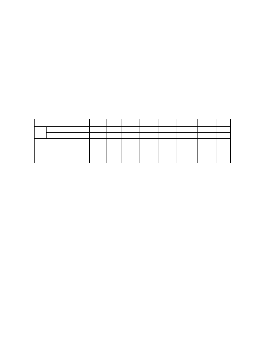
Table 22: Bus Operations Summary
Bus Operation
RST#
CLK
ADV#
CE#
OE#
WE#
WAIT
DQ[15:0]
Notes
Read
Asynchronous
VIH
XL
L
H
Deasserted
Output
Synchronous
VIH
Running
L
H
Driven
Output
Write
VIH
X
L
H
L
High-Z
Input
1
Output Disable
VIH
X
L
H
High-Z
2
Standby
VIH
X
H
X
High-Z
2
Reset
VIL
X
High-Z
2,3
Notes:
1.
Refer to the
Table 23, “Command Bus Cycles” on page 45 for valid DQ[15:0] during a write
operation.
2.
X = Don’t Care (H or L).
3.
RST# must be at VSS ± 0.2 V to meet the maximum specified power-down current.
相关PDF资料 |
PDF描述 |
|---|---|
| RC28F160C3TC90 | 1M X 16 FLASH 3V PROM, 90 ns, PBGA64 |
| RC28F160C3BD70 | 1M X 16 FLASH 3V PROM, 70 ns, PBGA64 |
| RC4194K | DUAL OUTPUT, ADJUSTABLE MIXED REGULATOR, MBFM9 |
| RM4194K | DUAL OUTPUT, ADJUSTABLE MIXED REGULATOR, MBFM9 |
| RC4194D | DUAL OUTPUT, ADJUSTABLE MIXED REGULATOR, CDIP14 |
相关代理商/技术参数 |
参数描述 |
|---|---|
| RC28F256P33T85B | 制造商:Micron Technology Inc 功能描述:256MB, KEARNY EBGA 3.0 - Tape and Reel |
| RC28F256P33TFA | 功能描述:IC FLASH 256MBIT 95NS 64EZBGA RoHS:否 类别:集成电路 (IC) >> 存储器 系列:Axcell™ 产品变化通告:Product Discontinuation 26/Apr/2010 标准包装:136 系列:- 格式 - 存储器:RAM 存储器类型:SRAM - 同步,DDR II 存储容量:18M(1M x 18) 速度:200MHz 接口:并联 电源电压:1.7 V ~ 1.9 V 工作温度:0°C ~ 70°C 封装/外壳:165-TBGA 供应商设备封装:165-CABGA(13x15) 包装:托盘 其它名称:71P71804S200BQ |
| RC28F256P33TFE | 功能描述:IC FLASH 256MBIT 64EZBGA RoHS:否 类别:集成电路 (IC) >> 存储器 系列:Axcell™ 标准包装:72 系列:- 格式 - 存储器:RAM 存储器类型:SRAM - 同步 存储容量:4.5M(256K x 18) 速度:133MHz 接口:并联 电源电压:3.135 V ~ 3.465 V 工作温度:0°C ~ 70°C 封装/外壳:100-LQFP 供应商设备封装:100-TQFP(14x20) 包装:托盘 |
| RC28F320C3 | 制造商:INTEL 制造商全称:Intel Corporation 功能描述:3 VOLT ADVANCED+ BOOT BLOCK 8-, 16-, 32-MBIT FLASH MEMORY FAMILY |
| RC28F320C3BA100 | 功能描述:IC FLASH 32MBIT 100NS 64BGA RoHS:否 类别:集成电路 (IC) >> 存储器 系列:- 标准包装:150 系列:- 格式 - 存储器:EEPROMs - 串行 存储器类型:EEPROM 存储容量:4K (2 x 256 x 8) 速度:400kHz 接口:I²C,2 线串口 电源电压:2.5 V ~ 5.5 V 工作温度:-40°C ~ 85°C 封装/外壳:8-VFDFN 裸露焊盘 供应商设备封装:8-DFN(2x3) 包装:管件 产品目录页面:1445 (CN2011-ZH PDF) |
发布紧急采购,3分钟左右您将得到回复。