- 您现在的位置:买卖IC网 > PDF目录225025 > RC28F256P33T85A (NUMONYX) 16M X 16 FLASH 3V PROM, 85 ns, PBGA64 PDF资料下载
参数资料
| 型号: | RC28F256P33T85A |
| 厂商: | NUMONYX |
| 元件分类: | PROM |
| 英文描述: | 16M X 16 FLASH 3V PROM, 85 ns, PBGA64 |
| 封装: | BGA-64 |
| 文件页数: | 43/96页 |
| 文件大小: | 1378K |
| 代理商: | RC28F256P33T85A |
第1页第2页第3页第4页第5页第6页第7页第8页第9页第10页第11页第12页第13页第14页第15页第16页第17页第18页第19页第20页第21页第22页第23页第24页第25页第26页第27页第28页第29页第30页第31页第32页第33页第34页第35页第36页第37页第38页第39页第40页第41页第42页当前第43页第44页第45页第46页第47页第48页第49页第50页第51页第52页第53页第54页第55页第56页第57页第58页第59页第60页第61页第62页第63页第64页第65页第66页第67页第68页第69页第70页第71页第72页第73页第74页第75页第76页第77页第78页第79页第80页第81页第82页第83页第84页第85页第86页第87页第88页第89页第90页第91页第92页第93页第94页第95页第96页
Numonyx StrataFlash Embedded Memory (P33)
Datasheet
November 2007
48
Order Number: 314749-05
11.0
Device Operations
This section provides an overview of device operations. The system Central Processing
Unit provides control of all in-system read, write, and erase operations of the device via
the system bus. The on-chip WSM manages all block-erase and word-program
algorithms.
Device commands are written to the CUI to control all flash memory device operations.
The CUI does not occupy an addressable memory location; it is the mechanism through
which the flash device is controlled.
11.1
Status Register
To read the Status Register, issue the Read Status Register command at any address.
Status Register information is available to which the Read Status Register, Word
Program, or Block Erase command was issued. SRD is automatically made available
following a Word Program, Block Erase, or Block Lock command sequence. Reads from
the device after any of these command sequences outputs the device’s status until
another valid command is written (e.g. the Read Array command).
The Status Register is read using single asynchronous-mode or synchronous burst
mode reads. SRD is output on DQ[7:0], while 0x00 is output on DQ[15:8]. In
asynchronous mode the falling edge of OE#, or CE# (whichever occurs first) updates
and latches the Status Register contents. However, when reading the Status Register in
synchronous burst mode, CE# or ADV# must be toggled to update SRD.
The Device Write Status bit (SR[7]) provides overall status of the device. SR[6:1]
present status and error information about the program, erase, suspend, VPP, and
block-locked operations.
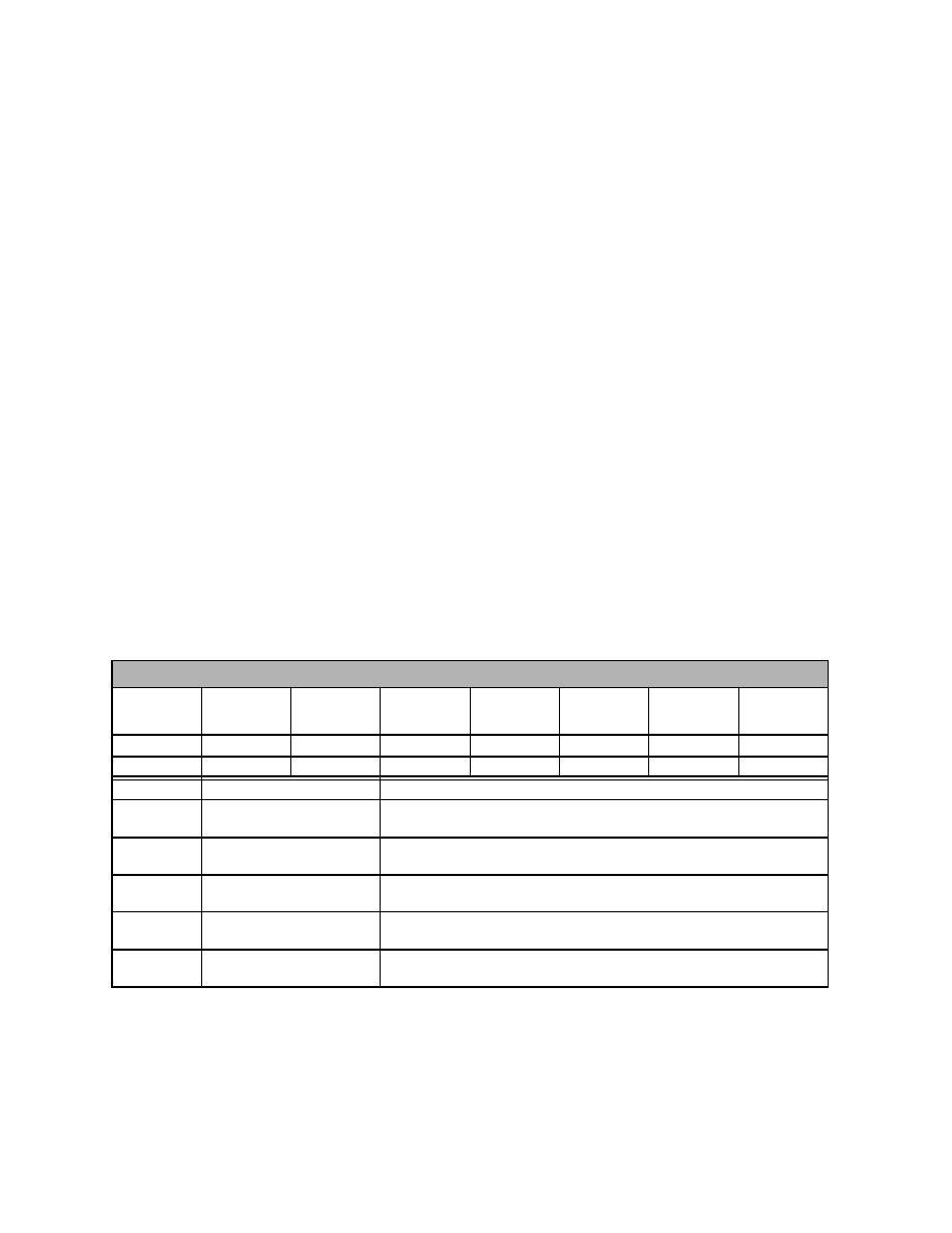
Table 25: Status Register Description (Sheet 1 of 2)
Status Register (SR)
Default Value = 0x80
Device Write
Status
Erase
Suspend
Status
Erase Status
Program
Status
VPP Status
Program
Suspend
Status
Block-Locked
Status
BEFP
Write
Status
DWS
ESS
ES
PS
VPPS
PSS
BLS
BWS
76
5432
10
Bit
Name
Description
7
Device Write Status (DWS)
0 = Device is busy; program or erase cycle in progress; SR[0] valid.
1 = Device is ready; SR[6:1] are valid.
6
Erase Suspend Status (ESS)
0 = Erase suspend not in effect.
1 = Erase suspend in effect.
5
Erase Status (ES)
0 = Erase successful.
1 = Erase fail or program sequence error when set with SR[4,7].
4
Program Status (PS)
0 = Program successful.
1 = Program fail or program sequence error when set with SR[5,7]
3VPP Status (VPPS)
0 = VPP within acceptable limits during program or erase operation.
1 = VPP < VPPLK during program or erase operation.
相关PDF资料 |
PDF描述 |
|---|---|
| RC28F160C3TC90 | 1M X 16 FLASH 3V PROM, 90 ns, PBGA64 |
| RC28F160C3BD70 | 1M X 16 FLASH 3V PROM, 70 ns, PBGA64 |
| RC4194K | DUAL OUTPUT, ADJUSTABLE MIXED REGULATOR, MBFM9 |
| RM4194K | DUAL OUTPUT, ADJUSTABLE MIXED REGULATOR, MBFM9 |
| RC4194D | DUAL OUTPUT, ADJUSTABLE MIXED REGULATOR, CDIP14 |
相关代理商/技术参数 |
参数描述 |
|---|---|
| RC28F256P33T85B | 制造商:Micron Technology Inc 功能描述:256MB, KEARNY EBGA 3.0 - Tape and Reel |
| RC28F256P33TFA | 功能描述:IC FLASH 256MBIT 95NS 64EZBGA RoHS:否 类别:集成电路 (IC) >> 存储器 系列:Axcell™ 产品变化通告:Product Discontinuation 26/Apr/2010 标准包装:136 系列:- 格式 - 存储器:RAM 存储器类型:SRAM - 同步,DDR II 存储容量:18M(1M x 18) 速度:200MHz 接口:并联 电源电压:1.7 V ~ 1.9 V 工作温度:0°C ~ 70°C 封装/外壳:165-TBGA 供应商设备封装:165-CABGA(13x15) 包装:托盘 其它名称:71P71804S200BQ |
| RC28F256P33TFE | 功能描述:IC FLASH 256MBIT 64EZBGA RoHS:否 类别:集成电路 (IC) >> 存储器 系列:Axcell™ 标准包装:72 系列:- 格式 - 存储器:RAM 存储器类型:SRAM - 同步 存储容量:4.5M(256K x 18) 速度:133MHz 接口:并联 电源电压:3.135 V ~ 3.465 V 工作温度:0°C ~ 70°C 封装/外壳:100-LQFP 供应商设备封装:100-TQFP(14x20) 包装:托盘 |
| RC28F320C3 | 制造商:INTEL 制造商全称:Intel Corporation 功能描述:3 VOLT ADVANCED+ BOOT BLOCK 8-, 16-, 32-MBIT FLASH MEMORY FAMILY |
| RC28F320C3BA100 | 功能描述:IC FLASH 32MBIT 100NS 64BGA RoHS:否 类别:集成电路 (IC) >> 存储器 系列:- 标准包装:150 系列:- 格式 - 存储器:EEPROMs - 串行 存储器类型:EEPROM 存储容量:4K (2 x 256 x 8) 速度:400kHz 接口:I²C,2 线串口 电源电压:2.5 V ~ 5.5 V 工作温度:-40°C ~ 85°C 封装/外壳:8-VFDFN 裸露焊盘 供应商设备封装:8-DFN(2x3) 包装:管件 产品目录页面:1445 (CN2011-ZH PDF) |
发布紧急采购,3分钟左右您将得到回复。