- 您现在的位置:买卖IC网 > PDF目录225025 > RC28F256P33T85A (NUMONYX) 16M X 16 FLASH 3V PROM, 85 ns, PBGA64 PDF资料下载
参数资料
| 型号: | RC28F256P33T85A |
| 厂商: | NUMONYX |
| 元件分类: | PROM |
| 英文描述: | 16M X 16 FLASH 3V PROM, 85 ns, PBGA64 |
| 封装: | BGA-64 |
| 文件页数: | 40/96页 |
| 文件大小: | 1378K |
| 代理商: | RC28F256P33T85A |
第1页第2页第3页第4页第5页第6页第7页第8页第9页第10页第11页第12页第13页第14页第15页第16页第17页第18页第19页第20页第21页第22页第23页第24页第25页第26页第27页第28页第29页第30页第31页第32页第33页第34页第35页第36页第37页第38页第39页当前第40页第41页第42页第43页第44页第45页第46页第47页第48页第49页第50页第51页第52页第53页第54页第55页第56页第57页第58页第59页第60页第61页第62页第63页第64页第65页第66页第67页第68页第69页第70页第71页第72页第73页第74页第75页第76页第77页第78页第79页第80页第81页第82页第83页第84页第85页第86页第87页第88页第89页第90页第91页第92页第93页第94页第95页第96页
November 2007
Datasheet
Order Number: 314749-05
45
Numonyx StrataFlash Embedded Memory (P33)
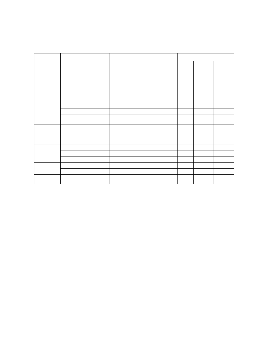
Table 23: Command Bus Cycles
Mode
Command
Bus
Cycles
First Bus Cycle
Second Bus Cycle
Oper
Addr(1)
Data(2)
Oper
Addr(1)
Data(2)
Read
Read Array
1
Write
DnA
0xFF
-
Read Device Identifier
≥ 2
Write
DnA
0x90
Read
DBA + IA
ID
CFI Query
≥ 2
Write
DnA
0x98
Read
DBA + QA
QD
Read Status Register
2
Write
DnA
0x70
Read
DnA
SRD
Clear Status Register
1
Write
DnA
0x50
-
Program
Word Program
2
Write
WA
0x40/
0x10
Write
WA
WD
Buffered Program(3)
> 2Write
WA
0xE8
Write
WA
N - 1
Buffered Enhanced Factory
Program (BEFP)(4)
> 2
Write
WA
0x80
Write
WA
0xD0
Erase
Block Erase
2
Write
BA
0x20
Write
BA
0xD0
Suspend
Program/Erase Suspend
1
Write
DnA
0xB0
-
Program/Erase Resume
1
Write
DnA
0xD0
-
Block
Locking/
Unlocking
Lock Block
2
Write
BA
0x60
Write
BA
0x01
Unlock Block
2
Write
BA
0x60
Write
BA
0xD0
Lock-down Block
2
Write
BA
0x60
Write
BA
0x2F
Protection
Program Protection Register
2
Write
PRA
0xC0
Write
PRA
PD
Program Lock Register
2
Write
LRA
0xC0
Write
LRA
LRD
Configuration Program Read Configuration
Register
2
Write
RCD
0x60
Write
RCD
0x03
Notes:
1.
First command cycle address should be the same as the operation’s target address.
DBA = Device Base Address (NOTE: needed for dual-die 512Mbit device)
DnA = Address within the device.
IA = Identification code address offset.
QA = CFI Query address offset.
WA = Word address of memory location to be written.
BA = Address within the block.
PRA = Protection Register address.
LRA = Lock Register address.
RCD = Read Configuration Register data on QUAD+ A[15:0] or EASY BGA / TSOP A[16:1].
2.
ID = Identifier data.
QD = Query data on DQ[15:0].
SRD = Status Register data.
WD = Word data.
N = Word count of data to be loaded into the write buffer.
PD = Protection Register data.
LRD = Lock Register data.
3.
The second cycle of the Buffered Program Command is the word count of the data to be loaded into the write buffer. This
is followed by up to 32 words of data.Then the confirm command (0xD0) is issued, triggering the array programming
operation.
4.
The confirm command (0xD0) is followed by the buffer data.
相关PDF资料 |
PDF描述 |
|---|---|
| RC28F160C3TC90 | 1M X 16 FLASH 3V PROM, 90 ns, PBGA64 |
| RC28F160C3BD70 | 1M X 16 FLASH 3V PROM, 70 ns, PBGA64 |
| RC4194K | DUAL OUTPUT, ADJUSTABLE MIXED REGULATOR, MBFM9 |
| RM4194K | DUAL OUTPUT, ADJUSTABLE MIXED REGULATOR, MBFM9 |
| RC4194D | DUAL OUTPUT, ADJUSTABLE MIXED REGULATOR, CDIP14 |
相关代理商/技术参数 |
参数描述 |
|---|---|
| RC28F256P33T85B | 制造商:Micron Technology Inc 功能描述:256MB, KEARNY EBGA 3.0 - Tape and Reel |
| RC28F256P33TFA | 功能描述:IC FLASH 256MBIT 95NS 64EZBGA RoHS:否 类别:集成电路 (IC) >> 存储器 系列:Axcell™ 产品变化通告:Product Discontinuation 26/Apr/2010 标准包装:136 系列:- 格式 - 存储器:RAM 存储器类型:SRAM - 同步,DDR II 存储容量:18M(1M x 18) 速度:200MHz 接口:并联 电源电压:1.7 V ~ 1.9 V 工作温度:0°C ~ 70°C 封装/外壳:165-TBGA 供应商设备封装:165-CABGA(13x15) 包装:托盘 其它名称:71P71804S200BQ |
| RC28F256P33TFE | 功能描述:IC FLASH 256MBIT 64EZBGA RoHS:否 类别:集成电路 (IC) >> 存储器 系列:Axcell™ 标准包装:72 系列:- 格式 - 存储器:RAM 存储器类型:SRAM - 同步 存储容量:4.5M(256K x 18) 速度:133MHz 接口:并联 电源电压:3.135 V ~ 3.465 V 工作温度:0°C ~ 70°C 封装/外壳:100-LQFP 供应商设备封装:100-TQFP(14x20) 包装:托盘 |
| RC28F320C3 | 制造商:INTEL 制造商全称:Intel Corporation 功能描述:3 VOLT ADVANCED+ BOOT BLOCK 8-, 16-, 32-MBIT FLASH MEMORY FAMILY |
| RC28F320C3BA100 | 功能描述:IC FLASH 32MBIT 100NS 64BGA RoHS:否 类别:集成电路 (IC) >> 存储器 系列:- 标准包装:150 系列:- 格式 - 存储器:EEPROMs - 串行 存储器类型:EEPROM 存储容量:4K (2 x 256 x 8) 速度:400kHz 接口:I²C,2 线串口 电源电压:2.5 V ~ 5.5 V 工作温度:-40°C ~ 85°C 封装/外壳:8-VFDFN 裸露焊盘 供应商设备封装:8-DFN(2x3) 包装:管件 产品目录页面:1445 (CN2011-ZH PDF) |
发布紧急采购,3分钟左右您将得到回复。