- 您现在的位置:买卖IC网 > PDF目录225025 > RC28F256P33T85A (NUMONYX) 16M X 16 FLASH 3V PROM, 85 ns, PBGA64 PDF资料下载
参数资料
| 型号: | RC28F256P33T85A |
| 厂商: | NUMONYX |
| 元件分类: | PROM |
| 英文描述: | 16M X 16 FLASH 3V PROM, 85 ns, PBGA64 |
| 封装: | BGA-64 |
| 文件页数: | 49/96页 |
| 文件大小: | 1378K |
| 代理商: | RC28F256P33T85A |
第1页第2页第3页第4页第5页第6页第7页第8页第9页第10页第11页第12页第13页第14页第15页第16页第17页第18页第19页第20页第21页第22页第23页第24页第25页第26页第27页第28页第29页第30页第31页第32页第33页第34页第35页第36页第37页第38页第39页第40页第41页第42页第43页第44页第45页第46页第47页第48页当前第49页第50页第51页第52页第53页第54页第55页第56页第57页第58页第59页第60页第61页第62页第63页第64页第65页第66页第67页第68页第69页第70页第71页第72页第73页第74页第75页第76页第77页第78页第79页第80页第81页第82页第83页第84页第85页第86页第87页第88页第89页第90页第91页第92页第93页第94页第95页第96页
November 2007
Datasheet
Order Number: 314749-05
53
Numonyx StrataFlash Embedded Memory (P33)
11.1.0.6
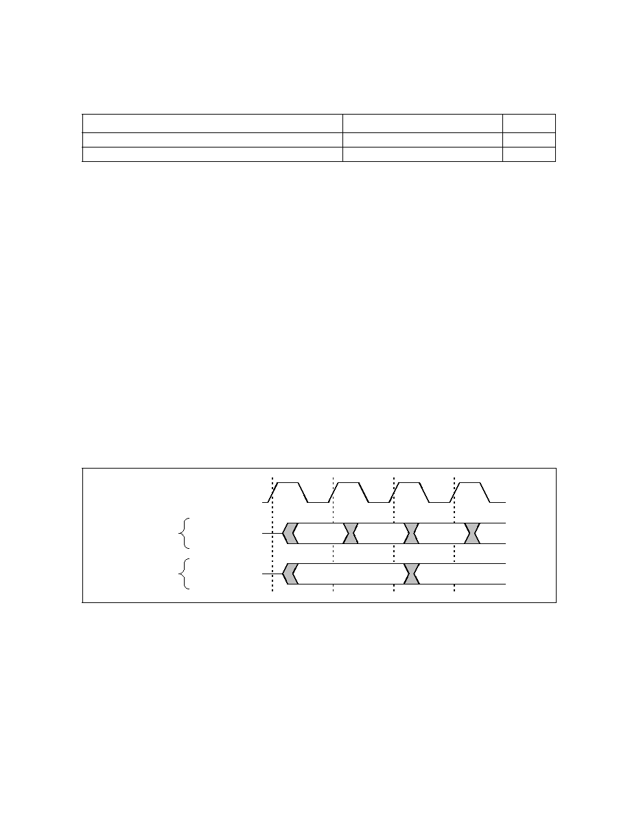
Data Hold
For burst read operations, the Data Hold (DH) bit determines whether the data output
remains valid on DQ[15:0] for one or two clock cycles. This period of time is called the
“data cycle”. When DH is set, output data is held for two clocks (default). When DH is
cleared, output data is held for one clock (see Figure 29). The processor’s data setup
time and the flash memory’s clock-to-data output delay should be considered when
determining whether to hold output data for one or two clocks. A method for
determining the DH configuration is shown below:
To set the device at one clock data hold for subsequent reads, the following condition
must be satisfied:
tCHQV (ns) + tDATA (ns) ≤ One CLK Period (ns)
tDATA = Data set up to Clock (defined by CPU)
For example, with a clock frequency of 40 MHz, the clock period is 25 ns. Assuming
tCHQV = 20 ns and tDATA = 4 ns. Applying these values to the formula above:
20 ns + 4 ns ≤ 25 ns
The equation is satisfied and data will be available at every clock period with data hold
setting at one clock. If tCHQV (ns) + tDATA (ns) > One CLK Period (ns), data hold setting of
2 clock periods must be used.
11.1.0.7
WAIT Delay
The WAIT Delay (WD) bit controls the WAIT assertion-delay behavior during
synchronous burst reads. WAIT can be asserted either during or one data cycle before
valid data is output on DQ[15:0]. When WD is set, WAIT is deasserted one data cycle
before valid data (default). When WD is cleared, WAIT is deasserted during valid data.
All Asynchronous Reads
Deasserted
1
All Writes
High-Z
1,2
Notes:
1.
Active: WAIT is asserted until data becomes valid, then deasserts.
2.
When OE# = VIH during writes, WAIT = High-Z.
Table 28: WAIT Functionality Table (Sheet 2 of 2)
Condition
WAIT
Notes
Figure 29: Data Hold Timing
Valid
Output
Valid
Output
Valid
Output
Valid
Output
Valid
Output
CLK [C]
D[15:0] [Q]
2 CLK
Data Hold
1 CLK
Data Hold
相关PDF资料 |
PDF描述 |
|---|---|
| RC28F160C3TC90 | 1M X 16 FLASH 3V PROM, 90 ns, PBGA64 |
| RC28F160C3BD70 | 1M X 16 FLASH 3V PROM, 70 ns, PBGA64 |
| RC4194K | DUAL OUTPUT, ADJUSTABLE MIXED REGULATOR, MBFM9 |
| RM4194K | DUAL OUTPUT, ADJUSTABLE MIXED REGULATOR, MBFM9 |
| RC4194D | DUAL OUTPUT, ADJUSTABLE MIXED REGULATOR, CDIP14 |
相关代理商/技术参数 |
参数描述 |
|---|---|
| RC28F256P33T85B | 制造商:Micron Technology Inc 功能描述:256MB, KEARNY EBGA 3.0 - Tape and Reel |
| RC28F256P33TFA | 功能描述:IC FLASH 256MBIT 95NS 64EZBGA RoHS:否 类别:集成电路 (IC) >> 存储器 系列:Axcell™ 产品变化通告:Product Discontinuation 26/Apr/2010 标准包装:136 系列:- 格式 - 存储器:RAM 存储器类型:SRAM - 同步,DDR II 存储容量:18M(1M x 18) 速度:200MHz 接口:并联 电源电压:1.7 V ~ 1.9 V 工作温度:0°C ~ 70°C 封装/外壳:165-TBGA 供应商设备封装:165-CABGA(13x15) 包装:托盘 其它名称:71P71804S200BQ |
| RC28F256P33TFE | 功能描述:IC FLASH 256MBIT 64EZBGA RoHS:否 类别:集成电路 (IC) >> 存储器 系列:Axcell™ 标准包装:72 系列:- 格式 - 存储器:RAM 存储器类型:SRAM - 同步 存储容量:4.5M(256K x 18) 速度:133MHz 接口:并联 电源电压:3.135 V ~ 3.465 V 工作温度:0°C ~ 70°C 封装/外壳:100-LQFP 供应商设备封装:100-TQFP(14x20) 包装:托盘 |
| RC28F320C3 | 制造商:INTEL 制造商全称:Intel Corporation 功能描述:3 VOLT ADVANCED+ BOOT BLOCK 8-, 16-, 32-MBIT FLASH MEMORY FAMILY |
| RC28F320C3BA100 | 功能描述:IC FLASH 32MBIT 100NS 64BGA RoHS:否 类别:集成电路 (IC) >> 存储器 系列:- 标准包装:150 系列:- 格式 - 存储器:EEPROMs - 串行 存储器类型:EEPROM 存储容量:4K (2 x 256 x 8) 速度:400kHz 接口:I²C,2 线串口 电源电压:2.5 V ~ 5.5 V 工作温度:-40°C ~ 85°C 封装/外壳:8-VFDFN 裸露焊盘 供应商设备封装:8-DFN(2x3) 包装:管件 产品目录页面:1445 (CN2011-ZH PDF) |
发布紧急采购,3分钟左右您将得到回复。