- 您现在的位置:买卖IC网 > PDF目录69322 > RK80532RC056128 (INTEL CORP) 2400 MHz, MICROPROCESSOR, CPGA478 PDF资料下载
参数资料
| 型号: | RK80532RC056128 |
| 厂商: | INTEL CORP |
| 元件分类: | 微控制器/微处理器 |
| 英文描述: | 2400 MHz, MICROPROCESSOR, CPGA478 |
| 封装: | FLIP CHIP, PGA2-478 |
| 文件页数: | 11/99页 |
| 文件大小: | 4142K |
| 代理商: | RK80532RC056128 |
第1页第2页第3页第4页第5页第6页第7页第8页第9页第10页当前第11页第12页第13页第14页第15页第16页第17页第18页第19页第20页第21页第22页第23页第24页第25页第26页第27页第28页第29页第30页第31页第32页第33页第34页第35页第36页第37页第38页第39页第40页第41页第42页第43页第44页第45页第46页第47页第48页第49页第50页第51页第52页第53页第54页第55页第56页第57页第58页第59页第60页第61页第62页第63页第64页第65页第66页第67页第68页第69页第70页第71页第72页第73页第74页第75页第76页第77页第78页第79页第80页第81页第82页第83页第84页第85页第86页第87页第88页第89页第90页第91页第92页第93页第94页第95页第96页第97页第98页第99页
Datasheet
19
Electrical Specifications
2.6
System Bus Signal Groups
To simplify the following discussion, the system bus signals have been combined into groups by
buffer type. AGTL+ input signals have differential input buffers that use GTLREF as a reference
level. In this document, the term “AGTL+ Input” refers to the AGTL+ input group as well as the
AGTL+ I/O group when receiving. Similarly, “AGTL+ Output” refers to the AGTL+ output group
as well as the AGTL+ I/O group when driving.
With the implementation of a source synchronous data bus, there is a need to specify two sets of
timing parameters. One set is for common clock signals which are dependent upon the rising edge
of BCLK0 (ADS#, HIT#, HITM#, etc.), and the second set is for the source synchronous signals
that are relative to their respective strobe lines (data and address) as well as the rising edge of
BCLK0. Asychronous signals are still present (A20M#, IGNNE#, etc.) and can become active at
any time during the clock cycle. Table 4 identifies which signals are common clock, source
synchronous, and asynchronous.
NOTES:
1. Refer to Section 5.2 for signal descriptions.
2. These AGTL+ signals do not have on-die termination. Refer to Section 2.5 and the appropriate Platform
Design Guide listed in Table 1 for termination requirements and further details.
3. In processor systems where there is no debug port implemented on the system board, these signals are used
to support a debug port interposer. In systems with the debug port implemented on the system board, these
signals are no connects.
4. These signal groups are not terminated by the processor. Refer to Section 2.5, the ITP700 Debug Port
Design Guide
, and the appropriate Platform Design Guide listed in Table 1 for termination requirements and
further details.
5. The value of these pins during the active-to-inactive edge of RESET# defines the processor configuration
options. See Section 7.1 for details.
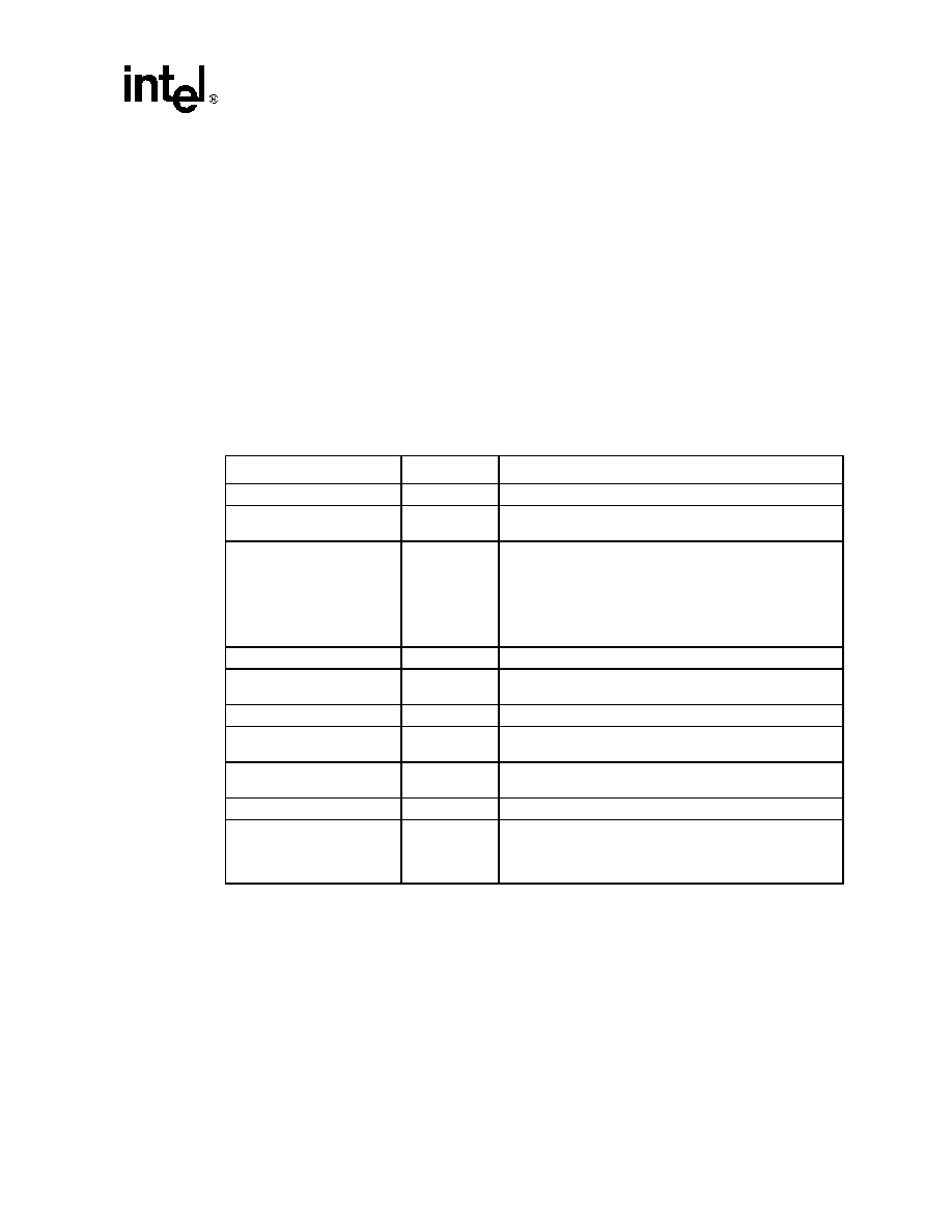
Table 4.
System Bus Pin Groups
Signal Group
Type
Signals1
AGTL+ Common Clock Input
Common Clock
BPRI#, DEFER#, RESET#2, RS[2:0]#, RSP#, TRDY#
AGTL+ Common Clock I/O
Synchronous
AP[1:0]#, ADS#, BINIT#, BNR#, BPM[5:0]#2, BR0#2,
DBSY#, DP[3:0]#, DRDY#, HIT#, HITM#, LOCK#, MCERR#
AGTL+ Source Synchronous
I/O
Source
Synchronous
Signals
Associated Strobe
REQ[4:0]#, A[16:3]#5
ADSTB0#
A[35:17]#5
ADSTB1#
D[15:0]#, DBI0#
DSTBP0#, DSTBN0#
D[31:16]#, DBI1#
DSTBP1#, DSTBN1#
D[47:32]#, DBI2#
DSTBP2#, DSTBN2#
D[63:48]#, DBI3#
DSTBP3#, DSTBN3#
AGTL+ Strobes
Common Clock
ADSTB[1:0]#, DSTBP[3:0]#, DSTBN[3:0]#
Asynchronous GTL+ Input 4, 5
Asynchronous
A20M#, IGNNE#, INIT#, LINT0/INTR, LINT1/NMI, SMI#,
SLP#, STPCLK#
Asynchronous GTL+ Output 4
Asynchronous
FERR#, IERR#, THERMTRIP#, PROCHOT#
TAP Input 4
Synchronous
to TCK
TCK, TDI, TMS, TRST#
TAP Output 4
Synchronous
to TCK
TDO
System Bus Clock
N/A
BCLK[1:0], ITP_CLK[1:0]3
Power/Other
N/A
VCC, VCCA, VCCIOPLL, VCCVID, VID[4:0], VSS, VSSA,
GTLREF[3:0], COMP[1:0], RESERVED, TESTHI[5:0, 12:8],
ITPCLKOUT[1:0], THERMDA, THERMDC, PWRGOOD,
SKTOCC#, VCC_SENSE, VSS_SENSE, BSEL[1:0], DBR#
3
相关PDF资料 |
PDF描述 |
|---|---|
| RK80546KG0882MM | 64-BIT, 3200 MHz, MICROPROCESSOR, CPGA604 |
| RK80546KG1042MM | 64-BIT, 3600 MHz, MICROPROCESSOR, CPGA604 |
| RK80546KG0802MM | 64-BIT, 3000 MHz, MICROPROCESSOR, CPGA604 |
| RK80546PG0801M | 32-BIT, 3000 MHz, MICROPROCESSOR, CPGA478 |
| RK80546PE0721M | 32-BIT, 2800 MHz, MICROPROCESSOR, CPGA478 |
相关代理商/技术参数 |
参数描述 |
|---|---|
| RK80532RC060128S L6ZY | 制造商:Intel 功能描述:MPU Celeron? Processor 0.13um 2.5GHz 478-Pin FCPGA2 制造商:Intel 功能描述:NORTHWOOD; MPU CELERON 0.13UM 2.5GHZ 478PIN FCPGA2 - Trays |
| RK80532RC060128SL72B | 功能描述:IC CELERON 2.5GHZ 478FC-PGA2 RoHS:否 类别:集成电路 (IC) >> 嵌入式 - 微处理器 系列:- 标准包装:2 系列:MPC8xx 处理器类型:32-位 MPC8xx PowerQUICC 特点:- 速度:133MHz 电压:3.3V 安装类型:表面贴装 封装/外壳:357-BBGA 供应商设备封装:357-PBGA(25x25) 包装:托盘 |
| RK80532RC064128 | 制造商:Rochester Electronics LLC 功能描述:- Bulk |
| RK805346RE067256 | 制造商:Intel 功能描述:TRAY CELERON D 330 - Trays |
| RK80546KF0871M | 制造商:Rochester Electronics LLC 功能描述:- Bulk |
发布紧急采购,3分钟左右您将得到回复。