- 您现在的位置:买卖IC网 > PDF目录69322 > RK80532RC056128 (INTEL CORP) 2400 MHz, MICROPROCESSOR, CPGA478 PDF资料下载
参数资料
| 型号: | RK80532RC056128 |
| 厂商: | INTEL CORP |
| 元件分类: | 微控制器/微处理器 |
| 英文描述: | 2400 MHz, MICROPROCESSOR, CPGA478 |
| 封装: | FLIP CHIP, PGA2-478 |
| 文件页数: | 36/99页 |
| 文件大小: | 4142K |
| 代理商: | RK80532RC056128 |
第1页第2页第3页第4页第5页第6页第7页第8页第9页第10页第11页第12页第13页第14页第15页第16页第17页第18页第19页第20页第21页第22页第23页第24页第25页第26页第27页第28页第29页第30页第31页第32页第33页第34页第35页当前第36页第37页第38页第39页第40页第41页第42页第43页第44页第45页第46页第47页第48页第49页第50页第51页第52页第53页第54页第55页第56页第57页第58页第59页第60页第61页第62页第63页第64页第65页第66页第67页第68页第69页第70页第71页第72页第73页第74页第75页第76页第77页第78页第79页第80页第81页第82页第83页第84页第85页第86页第87页第88页第89页第90页第91页第92页第93页第94页第95页第96页第97页第98页第99页
Datasheet
41
System Bus Signal Quality Specifications
3.0
System Bus Signal Quality Specifications
Source synchronous data transfer requires the clean reception of data signals and their associated
strobes. Ringing below receiver thresholds, non-monotonic signal edges, and excessive voltage
swing will adversely affect system timings. Ringback and signal non-monotinicity cannot be
tolerated since these phenomena may inadvertently advance receiver state machines. Excessive
signal swings (overshoot and undershoot) are detrimental to silicon gate oxide integrity, and can
cause device failure if absolute voltage limits are exceeded. Additionally, overshoot and
undershoot can cause timing degradation due to the build up of inter-symbol interference (ISI)
effects. For these reasons, it is important that the designer work to achieve a solution that provides
acceptable signal quality across all systematic variations encountered in volume manufacturing.
This section documents signal quality metrics used to derive topology and routing guidelines
through simulation and for interpreting results for signal quality measurements of actual designs.
3.1
System Bus Clock (BCLK) Signal Quality Specifications
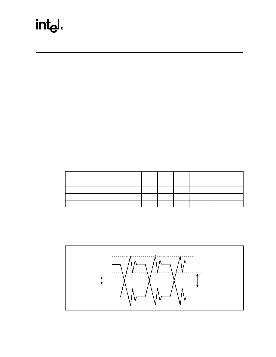
Table 23 describes the signal quality specifications at the processor core silicon for the processor
system bus clock (BCLK) signals. Figure 21 describes the signal quality waveform for the system
bus clock at the processor core silicon.
NOTES:
1. Unless otherwise noted, all specifications in this table apply to all Celeron processor on 0.13 micron process
frequencies.
2. The rising and falling edge ringback voltage specified is the minimum (rising) or maximum (falling) absolute
voltage the BCLK signal can dip back to after passing the VIH (rising) or VIL (falling) voltage limits. This
specification is an absolute value.
Table 23. BCLK Signal Quality Specifications
Parameter
Min
Max
Unit
Figure
Notes1
BCLK[1:0] Overshoot
N/A
0.30
V
BCLK[1:0] Undershoot
N/A
0.30
V
BCLK[1:0] Ringback Margin
0.20
N/A
V
2
BCLK[1:0] Threshold Region
N/A
0.10
V
Figure 21. BCLK Signal Integrity Waveform
Crossing
Voltage
Threshold
Region
VH
VL
Overshoot
Undershoot
Ringback
Margin
Rising Edge
Ringback
Falling Edge
Ringback,
BCLK0
BCLK1
Crossing
Voltage
相关PDF资料 |
PDF描述 |
|---|---|
| RK80546KG0882MM | 64-BIT, 3200 MHz, MICROPROCESSOR, CPGA604 |
| RK80546KG1042MM | 64-BIT, 3600 MHz, MICROPROCESSOR, CPGA604 |
| RK80546KG0802MM | 64-BIT, 3000 MHz, MICROPROCESSOR, CPGA604 |
| RK80546PG0801M | 32-BIT, 3000 MHz, MICROPROCESSOR, CPGA478 |
| RK80546PE0721M | 32-BIT, 2800 MHz, MICROPROCESSOR, CPGA478 |
相关代理商/技术参数 |
参数描述 |
|---|---|
| RK80532RC060128S L6ZY | 制造商:Intel 功能描述:MPU Celeron? Processor 0.13um 2.5GHz 478-Pin FCPGA2 制造商:Intel 功能描述:NORTHWOOD; MPU CELERON 0.13UM 2.5GHZ 478PIN FCPGA2 - Trays |
| RK80532RC060128SL72B | 功能描述:IC CELERON 2.5GHZ 478FC-PGA2 RoHS:否 类别:集成电路 (IC) >> 嵌入式 - 微处理器 系列:- 标准包装:2 系列:MPC8xx 处理器类型:32-位 MPC8xx PowerQUICC 特点:- 速度:133MHz 电压:3.3V 安装类型:表面贴装 封装/外壳:357-BBGA 供应商设备封装:357-PBGA(25x25) 包装:托盘 |
| RK80532RC064128 | 制造商:Rochester Electronics LLC 功能描述:- Bulk |
| RK805346RE067256 | 制造商:Intel 功能描述:TRAY CELERON D 330 - Trays |
| RK80546KF0871M | 制造商:Rochester Electronics LLC 功能描述:- Bulk |
发布紧急采购,3分钟左右您将得到回复。