- 您现在的位置:买卖IC网 > PDF目录19483 > ADSP-21375KSWZ-2B (Analog Devices Inc)IC DSP 32BIT 266MHZ 208-MQFP PDF资料下载
参数资料
| 型号: | ADSP-21375KSWZ-2B |
| 厂商: | Analog Devices Inc |
| 文件页数: | 7/56页 |
| 文件大小: | 0K |
| 描述: | IC DSP 32BIT 266MHZ 208-MQFP |
| 产品培训模块: | SHARC Processor Overview |
| 标准包装: | 36 |
| 系列: | SHARC® |
| 类型: | 浮点 |
| 接口: | DAI,DPI |
| 时钟速率: | 266MHz |
| 非易失内存: | ROM(256 kB) |
| 芯片上RAM: | 64kB |
| 电压 - 输入/输出: | 3.30V |
| 电压 - 核心: | 1.20V |
| 工作温度: | 0°C ~ 70°C |
| 安装类型: | 表面贴装 |
| 封装/外壳: | 208-LQFP 裸露焊盘 |
| 供应商设备封装: | 208-LQFP-EP(28x28) |
| 包装: | 托盘 |
第1页第2页第3页第4页第5页第6页当前第7页第8页第9页第10页第11页第12页第13页第14页第15页第16页第17页第18页第19页第20页第21页第22页第23页第24页第25页第26页第27页第28页第29页第30页第31页第32页第33页第34页第35页第36页第37页第38页第39页第40页第41页第42页第43页第44页第45页第46页第47页第48页第49页第50页第51页第52页第53页第54页第55页第56页
�� �
�
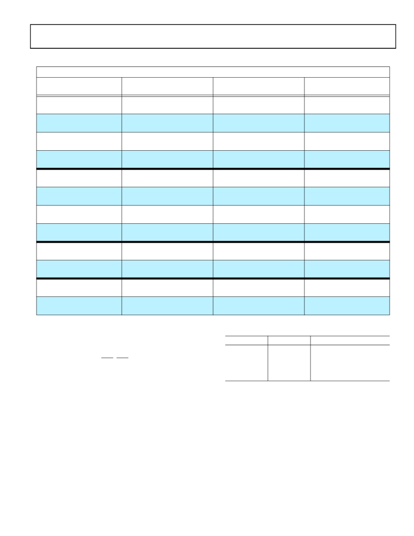
�ADSP-21371� /� ADSP-21375�
�Table� 4.� ADSP-21375� Internal� Memory� Space�
�IOP� Registers� 0x0000� 0000–0x0003� FFFF�
�Extended� Precision� Normal� or�
�Long� Word� (64� bits)�
�BLOCK� 0� ROM�
�0x0004� 0000–0x0004� 3FFF�
�Reserved�
�0x0004� 4000–0x0004� BFFF�
�BLOCK� 0� RAM�
�0x0004� C000–0x0004� C7FF�
�Reserved�
�0x0004� C800–0x0004� FFFF�
�BLOCK� 1� ROM�
�0x0005� 0000–0x0005� 3FFF�
�Reserved�
�0x0005� 4000–0x0005� BFFF�
�BLOCK� 1� RAM�
�0x0005� C000–0x0005� C7FF�
�Reserved�
�0x0005� C800–0x0005� FFFF�
�BLOCK� 2� RAM�
�0x0006� 0000–0x0006� 07FF�
�Reserved�
�0x0006� 0800–0x0006� FFFF�
�BLOCK� 3� RAM�
�0x0007� 0000–0x0007� 07FF�
�Reserved�
�0x0007� 0800–0x0007� FFFF�
�Instruction� Word� (48� bits)�
�BLOCK� 0� ROM�
�0x0008� 0000–0x0008� 5554�
�Reserved�
�0x0008� 5555–0x0008� FFFF�
�BLOCK� 0� RAM�
�0x0009� 0000–0x0009� 0AA9�
�Reserved�
�0x0009� 0AAA–0x0009� FFFF�
�BLOCK� 1� ROM�
�0x000A� 0000–0x000A� 5554�
�Reserved�
�0x000A� 5555–0x000A� FFFF�
�BLOCK� 1� RAM�
�0x000B� 0000–0x000B� 0AA9�
�Reserved�
�0x000B� 0AAA–0x000B� FFFF�
�BLOCK� 2� RAM�
�0x000C� 0000–0x000C� 0AA9�
�Reserved�
�0x000C� 0AAA–0x000D� FFFF�
�BLOCK� 3� RAM�
�0x000E� 0000–0x000E� 0AA9�
�Reserved�
�0x000E� 0AAA–0x000F� FFFF�
�Normal� Word� (32� bits)�
�BLOCK� 0� ROM�
�0x0008� 0000–0x0008� 7FFF�
�Reserved�
�0x0008� 8000–0x0009� 7FFF�
�BLOCK� 0� RAM�
�0x0009� 8000–0x0009� 8FFF�
�Reserved�
�0x0009� 9000–0x0009� FFFF�
�BLOCK� 1� ROM�
�0x000A� 0000–0x000A� 7FFF�
�Reserved�
�0x000A� 8000–0x000B� 7FFF�
�BLOCK� 1� RAM�
�0x000B� 8000–0x000B� 8FFF�
�Reserved�
�0x000B� 9000–0x000B� FFFF�
�BLOCK� 2� RAM�
�0x000C� 0000–0x000C� 0FFF�
�Reserved�
�0x000C� 1000–0x000D� FFFF�
�BLOCK� 3� RAM�
�0x000E� 0000–0x000E� 0FFF�
�Reserved�
�0x000E� 1000–0x000F� FFFF�
�Short� Word� (16� bits)�
�BLOCK� 0� ROM�
�0x0010� 0000–0x0010� FFFF�
�Reserved�
�0x0011� 0000–0x0012� FFFF�
�BLOCK� 0� RAM�
�0x0013� 0000–0x0013� 1FFF�
�Reserved�
�0x0013� 2000–0x0013� FFFF�
�BLOCK� 1� ROM�
�0x0014� 0000–0x0014� FFFF�
�Reserved�
�0x0015� 0000–0x0016� FFFF�
�BLOCK� 1� RAM�
�0x0017� 0000–0x0017� 1FFF�
�Reserved�
�0x0017� 2000–0x0017� FFFF�
�BLOCK� 2� RAM�
�0x0018� 0000–0x0018� 1FFF�
�Reserved�
�0x0018� 2000–0x001B� FFFF�
�BLOCK� 3� RAM�
�0x001C� 0000–0x001C� 1FFF�
�Reserved�
�0x001C� 2000–0x001F� FFFF�
�SDRAM� Controller�
�Table� 5.� External� Memory� for� SDRAM� Addresses�
�The� SDRAM� controller� provides� an� interface� to� up� to� four� sepa-�
�rate� banks� of� industry-standard� SDRAM� devices� or� DIMMs.�
�Fully� compliant� with� the� SDRAM� standard,� each� bank� has� its�
�own� memory� select� line� (MS0–MS3),� and� can� be� configured� to�
�contain� between� 16M� bytes� and� 256M� bytes� of� memory.�
��Bank�
�Bank� 0�
�Bank� 1�
�Bank� 2�
�Bank� 3�
�Size� in� Words�
�62M�
�64M�
�64M�
�64M�
�Address� Range�
�0x0020� 0000–0x03FF� FFFF�
�0x0400� 0000–0x07FF� FFFF�
�0x0800� 0000–0x0BFF� FFFF�
�0x0C00� 0000–0x0FFF� FFFF�
�The� controller� maintains� all� of� the� banks� as� a� contiguous�
�address� space� so� that� the� processor� sees� this� as� a� single� address�
�space,� even� if� different� size� devices� are� used� in� the�
�different� banks.�
�A� set� of� programmable� timing� parameters� is� available� to� config-�
�ure� the� SDRAM� banks� to� support� slower� memory� devices.� The�
�memory� banks� can� be� configured� as� 16� bits� wide� or� as�
�32� bits� wide.� The� SDRAM� controller� address,� data,� clock,� and�
�command� pins� can� drive� loads� up� to� 30� pF.� For� larger� memory�
�systems,� the� SDRAM� controller� external� buffer� timing� should�
�be� selected� and� external� buffering� should� be� provided� so� that� the�
�load� on� the� SDRAM� controller� pins� does� not� exceed� 30� pF.�
��are� for� normal� word� accesses.� If� 48-bit� instructions� are� placed� in�
�any� such� bank� (with� two� instructions� packed� into� three� 32-bit�
�locations),� then� care� must� be� taken� to� map� data� buffers� in� the�
�same� bank.� For� example,� if� 2k� instructions� are� placed� starting� at�
�the� bank� 0� base� address� (0x0020� 0000),� then� the� data� buffers� can�
�be� placed� starting� at� an� address� that� is� offset� by� 3k� words�
�(0x0020� 0C00).�
�External� Memory� Code� Execution�
�The� program� sequencer� can� execute� code� directly� from� external�
�memory� bank� 0� (SRAM,� SDRAM)� over� the� 48-bit� external� port�
�data� bus� (EPD).� This� allows� a� reduction� in� internal� memory�
�size,� thereby� reducing� the� die� area.� Because� instructions� on� the�
�Rev.� D� |� Page� 7� of� 56� |� April� 2013�
�相关PDF资料 |
PDF描述 |
|---|---|
| EEM06DRKH | CONN EDGECARD 12POS DIP .156 SLD |
| SMK316B7682KF-T | CAP CER 6800PF 630V 10% X7R 1206 |
| ECC22DCAH | CONN EDGECARD 44POS R/A .100 SLD |
| XC95144XL-5TQ100C | IC CPLD 144 MCELL 3.3V 100-TQFP |
| VE-20F-CY-F2 | CONVERTER MOD DC/DC 72V 50W |
相关代理商/技术参数 |
参数描述 |
|---|---|
| ADSP-21375KSWZ-2B2 | 制造商:AD 制造商全称:Analog Devices 功能描述:SHARC Processor optimized for high performance audio processing |
| ADSP-21375KSWZ-2BX | 制造商:Analog Devices 功能描述:- Trays |
| ADSP-21375KSZ-2B | 制造商:Analog Devices 功能描述:DSP FLOATING PT 32BIT/40-BIT 266MHZ 266MIPS 208MQFP - Trays |
| ADSP-21375KSZ-2BX | 制造商:Analog Devices 功能描述:266 MHZ.PROC W/ON CHIPROM,S/PDIF PBFREE - Trays |
| ADSP-21375KSZ-ENG | 制造商:AD 制造商全称:Analog Devices 功能描述:SHARC Processor |
发布紧急采购,3分钟左右您将得到回复。