- 您现在的位置:买卖IC网 > PDF目录1917 > DSP56301VF100 (Freescale Semiconductor)IC DSP 24BIT FIXED-POINT 252-BGA PDF资料下载
参数资料
| 型号: | DSP56301VF100 |
| 厂商: | Freescale Semiconductor |
| 文件页数: | 24/124页 |
| 文件大小: | 0K |
| 描述: | IC DSP 24BIT FIXED-POINT 252-BGA |
| 产品变化通告: | DSP56301 Discontinuation 12/Nov/2009 |
| 标准包装: | 60 |
| 系列: | DSP563xx |
| 类型: | 定点 |
| 接口: | 主机接口,SSI,SCI |
| 时钟速率: | 100MHz |
| 非易失内存: | ROM(9 kB) |
| 芯片上RAM: | 24kB |
| 电压 - 输入/输出: | 3.30V |
| 电压 - 核心: | 3.30V |
| 工作温度: | -40°C ~ 100°C |
| 安装类型: | 表面贴装 |
| 封装/外壳: | 252-BGA |
| 供应商设备封装: | 252-MAPBGA(21x21) |
| 包装: | 托盘 |
第1页第2页第3页第4页第5页第6页第7页第8页第9页第10页第11页第12页第13页第14页第15页第16页第17页第18页第19页第20页第21页第22页第23页当前第24页第25页第26页第27页第28页第29页第30页第31页第32页第33页第34页第35页第36页第37页第38页第39页第40页第41页第42页第43页第44页第45页第46页第47页第48页第49页第50页第51页第52页第53页第54页第55页第56页第57页第58页第59页第60页第61页第62页第63页第64页第65页第66页第67页第68页第69页第70页第71页第72页第73页第74页第75页第76页第77页第78页第79页第80页第81页第82页第83页第84页第85页第86页第87页第88页第89页第90页第91页第92页第93页第94页第95页第96页第97页第98页第99页第100页第101页第102页第103页第104页第105页第106页第107页第108页第109页第110页第111页第112页第113页第114页第115页第116页第117页第118页第119页第120页第121页第122页第123页第124页
DSP56301 Technical Data, Rev. 10
1-8
Freescale Semiconductor
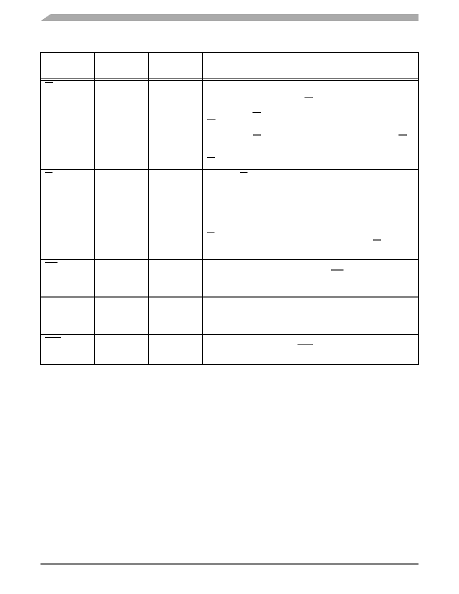
Signals/Connections
BB
Input/
Output
Input
Bus Busy
Indicates that the bus is active and must be asserted and deasserted
synchronous to CLKOUT. Only after BB is deasserted can the pending bus
master become the bus master (and then assert the signal again). The bus
master can keep BB asserted after ceasing bus activity, regardless of whether
BR is asserted or deasserted. This is called “bus parking” and allows the
current bus master to reuse the bus without re-arbitration until another device
requires the bus. BB is deasserted by an “active pull-up” method (that is, BB is
driven high and then released and held high by an external pull-up resistor).
BB requires an external pull-up resistor.
BL
Output
Driven high
(deasserted)
Bus Lock—BL is asserted at the start of an external divisible Read-Modify-
Write (RMW) bus cycle, remains asserted between the read and write cycles,
and is deasserted at the end of the write bus cycle. This provides an “early bus
start” signal for the bus controller. BL may be used to “resource lock” an
external multi-port memory for secure semaphore updates. Early deassertion
provides an “early bus end” signal useful for external bus control. If the
external bus is not used during an instruction cycle, BL remains deasserted
until the next external indivisible RMW cycle. The only instructions that assert
BL automatically are the BSET, CLR, and BCHG instructions when they are
used to modify external memory. An operation can also assert BL by setting
the BLH bit in the Bus Control Register.
CAS
Output
Tri-stated
Column Address Strobe
When the DSP is the bus master, DRAM uses CAS to strobe the column
address. Otherwise, if the Bus Mastership Enable (BME) bit in the DRAM
Control Register is cleared, the signal is tri-stated.
BCLK
Output
Tri-stated
Bus Clock
When the DSP is the bus master, BCLK is active when the OMR[ATE] is set.
When BCLK is active and synchronized to CLKOUT by the internal PLL, BCLK
precedes CLKOUT by one-fourth of a clock cycle.
BCLK
Output
Tri-stated
Bus Clock Not
When the DSP is the bus master, BCLK is the inverse of the BCLK signal.
Otherwise, the signal is tri-stated.
Table 1-8.
External Bus Control Signals (Continued)
Signal Name
Type
State During
Reset
Signal Description
相关PDF资料 |
PDF描述 |
|---|---|
| DSP56303VL100B1 | IC DSP 24BIT 100MHZ 196-BGA |
| DSP56311VF150B1 | IC DSP 24BIT 150MHZ 196-BGA |
| DSP56321VF200R2 | IC DSP 24BIT 200MHZ 196-BGA |
| DSP56852VFE | IC DSP 16BIT 120MHZ 81-MAPBGA |
| DSP56854FGE | IC DSP 16BIT 120MHZ 128-LQFP |
相关代理商/技术参数 |
参数描述 |
|---|---|
| DSP56301VF80 | 功能描述:数字信号处理器和控制器 - DSP, DSC MAP DSP RoHS:否 制造商:Microchip Technology 核心:dsPIC 数据总线宽度:16 bit 程序存储器大小:16 KB 数据 RAM 大小:2 KB 最大时钟频率:40 MHz 可编程输入/输出端数量:35 定时器数量:3 设备每秒兆指令数:50 MIPs 工作电源电压:3.3 V 最大工作温度:+ 85 C 封装 / 箱体:TQFP-44 安装风格:SMD/SMT |
| DSP56301VF80B1 | 功能描述:数字信号处理器和控制器 - DSP, DSC DSP56301VF80B1 RoHS:否 制造商:Microchip Technology 核心:dsPIC 数据总线宽度:16 bit 程序存储器大小:16 KB 数据 RAM 大小:2 KB 最大时钟频率:40 MHz 可编程输入/输出端数量:35 定时器数量:3 设备每秒兆指令数:50 MIPs 工作电源电压:3.3 V 最大工作温度:+ 85 C 封装 / 箱体:TQFP-44 安装风格:SMD/SMT |
| DSP56301VL100 | 制造商:FREESCALE 制造商全称:Freescale Semiconductor, Inc 功能描述:24-Bit Digital Signal Processor |
| DSP56301VL80 | 制造商:FREESCALE 制造商全称:Freescale Semiconductor, Inc 功能描述:24-Bit Digital Signal Processor |
| DSP56302 | 制造商:MOTOROLA 制造商全称:Motorola, Inc 功能描述:DSP56301 Digital Signal Processor |
发布紧急采购,3分钟左右您将得到回复。