- 您现在的位置:买卖IC网 > PDF目录1917 > DSP56301VF100 (Freescale Semiconductor)IC DSP 24BIT FIXED-POINT 252-BGA PDF资料下载
参数资料
| 型号: | DSP56301VF100 |
| 厂商: | Freescale Semiconductor |
| 文件页数: | 83/124页 |
| 文件大小: | 0K |
| 描述: | IC DSP 24BIT FIXED-POINT 252-BGA |
| 产品变化通告: | DSP56301 Discontinuation 12/Nov/2009 |
| 标准包装: | 60 |
| 系列: | DSP563xx |
| 类型: | 定点 |
| 接口: | 主机接口,SSI,SCI |
| 时钟速率: | 100MHz |
| 非易失内存: | ROM(9 kB) |
| 芯片上RAM: | 24kB |
| 电压 - 输入/输出: | 3.30V |
| 电压 - 核心: | 3.30V |
| 工作温度: | -40°C ~ 100°C |
| 安装类型: | 表面贴装 |
| 封装/外壳: | 252-BGA |
| 供应商设备封装: | 252-MAPBGA(21x21) |
| 包装: | 托盘 |
第1页第2页第3页第4页第5页第6页第7页第8页第9页第10页第11页第12页第13页第14页第15页第16页第17页第18页第19页第20页第21页第22页第23页第24页第25页第26页第27页第28页第29页第30页第31页第32页第33页第34页第35页第36页第37页第38页第39页第40页第41页第42页第43页第44页第45页第46页第47页第48页第49页第50页第51页第52页第53页第54页第55页第56页第57页第58页第59页第60页第61页第62页第63页第64页第65页第66页第67页第68页第69页第70页第71页第72页第73页第74页第75页第76页第77页第78页第79页第80页第81页第82页当前第83页第84页第85页第86页第87页第88页第89页第90页第91页第92页第93页第94页第95页第96页第97页第98页第99页第100页第101页第102页第103页第104页第105页第106页第107页第108页第109页第110页第111页第112页第113页第114页第115页第116页第117页第118页第119页第120页第121页第122页第123页第124页
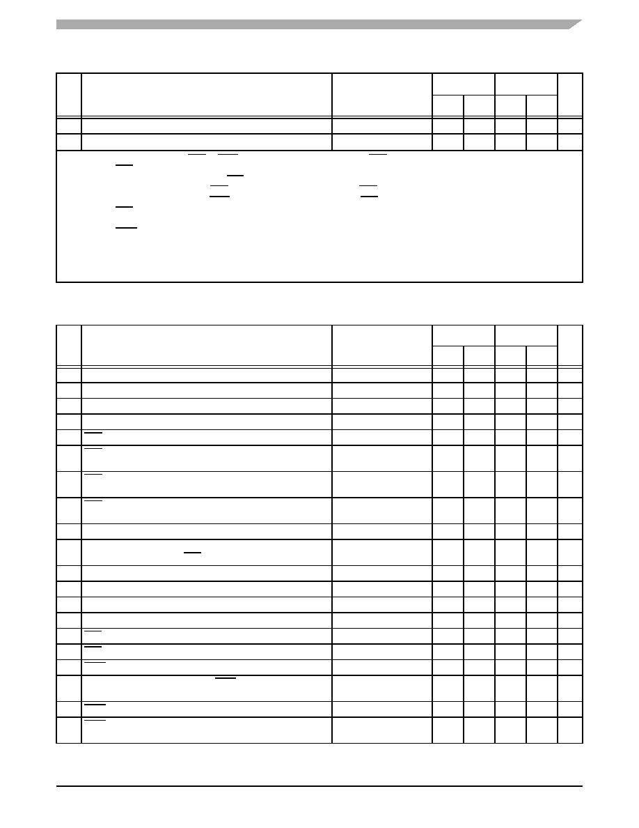
AC Electrical Characteristics
DSP56301 Technical Data, Rev. 10
Freescale Semiconductor
2-35
345
HDBDR High from Read Data Strobe Deassertion3
—
22.2
—
19.6
ns
346
HRST Assertion to Host Port Pins High Impedance2
—
22.2
—
19.6
ns
Notes:
1.
The Data Strobe is HRD or HWR in the Dual Data Strobe mode and HDS in the Single Data Strobe mode.
2.
HTA, HDRQ, and HRST may be programmed as active-high or active-low. In the example timing diagrams, HDRQ and HRST
are shown as active-high and HTA is shown as active low.
3.
The Read Data Strobe is HRD in the Dual Data Strobe mode and HDS in the Single Data Strobe mode.
4.
The Write Data Strobe is HWR in the Dual Data Strobe mode and HDS in the Single Data Strobe mode.
5.
HTA requires an external pull-down resistor if programmed as active high (HTAP = 0); or an external pull-up resistor if
programmed as active low (HTAP = 1). The resistor value should be consistent with the DC specifications.
6.
HIRQ requires an external pull-up resistor if programmed as open drain (HIRD = 0). The resistor value should be consistent
with the DC specifications.
7.
“LT” is the value of the latency timer register (CLAT) as programmed by the user during self configuration.
LT
≥ 1.
8.
Values are valid for VCC = 3.3 ± 0.3V
Table 2-19.
Universal Bus Mode, Synchronous Port A Type Host Timing
No.
Characteristic
Expression
80 MHz
100 MHz
Unit
Min
Max
Min
Max
300
Access Cycle Time
3
× TC
37.5
—
30.0
—
ns
301
HA[10–0], HAEN Setup to Data Strobe Assertion1
5.8
—
4.6
—
ns
302
HA[10–0], HAEN Valid Hold from Data Strobe Deassertion1
0.0
—
0.0
—
ns
305
Data Strobe Deasserted Width1
4.1
—
3.3
—
ns
307
HBS Asserted Pulse Width
2.5
—
2.0
—
ns
308
HBS Assertion to Data Strobe Assertion1
80 MHz: TC 4.9
100 MHz: TC 4.0
—7.6
—6.0
ns
309
HBS Assertion to Data Strobe Deassertion1
80 MHz: 2.5
× TC + 2.9
100 MHz: 2.5
× TC + 2.3
34.1
—
27.3
—
ns
310
HBS Deassertion to Data Strobe Deassertion1
80 MHz: 1.5
× TC + 3.3
100 MHz: 1.5
× TC + 2.6
22.1
—
17.6
—
ns
312
Data Out Active from Read Data Strobe Assertion3
1.7
—
1.3
—
ns
313
Data Out Valid from Read Data Strobe Assertion
(No Wait States Inserted—HTA Asserted)3
—
18.9
—
16.9
ns
314
Data Out Valid Hold from Read Data Strobe Deassertion3
1.7
—
1.3
—
ns
315
Data Out High Impedance from Read Data Strobe Deassertion3
—
12.0
—
9.6
ns
316
Data In Valid Setup to Write Data Strobe Deassertion4
8.3
—
6.6
—
ns
317
Data In Valid Hold from Write Data Strobe Deassertion4
0.0
—
0.0
—
ns
324
HTA Assertion to Data Strobe Deassertion1,2
0.0
—
0.0
—
ns
325
HTA High Impedance from Data Strobe Deassertion1,2
—
15.3
—
12.2
ns
326
HIRQ Asserted Pulse Width (HIRH = 0, HIRD = 1)
(LT + 1)
× TC 6.07
6.5
—
4.0
—
ns
327
Data Strobe Deasserted Hold from HIRQ Deassertion
(HIRH = 0)1
0.0
—
0.0
—
ns
328
HIRQ Asserted Hold from Data Strobe Assertion (HIRH = 1)1
1.5
× TC
18.8
—
15.0
—
ns
329
HIRQ Deassertion from Data Strobe Assertion
(HIRH = 1, HIRD = 1)1
80 MHz: 2.5
× TC + 24.7
100 MHz: 2.5
× TC + 21.5
—
55.9
—
46.5
ns
Table 2-18.
Universal Bus Mode Timing Parameters (Continued)
No.
Characteristic
Expression
80 MHz
100 MHz
Unit
Min
Max
Min
Max
相关PDF资料 |
PDF描述 |
|---|---|
| DSP56303VL100B1 | IC DSP 24BIT 100MHZ 196-BGA |
| DSP56311VF150B1 | IC DSP 24BIT 150MHZ 196-BGA |
| DSP56321VF200R2 | IC DSP 24BIT 200MHZ 196-BGA |
| DSP56852VFE | IC DSP 16BIT 120MHZ 81-MAPBGA |
| DSP56854FGE | IC DSP 16BIT 120MHZ 128-LQFP |
相关代理商/技术参数 |
参数描述 |
|---|---|
| DSP56301VF80 | 功能描述:数字信号处理器和控制器 - DSP, DSC MAP DSP RoHS:否 制造商:Microchip Technology 核心:dsPIC 数据总线宽度:16 bit 程序存储器大小:16 KB 数据 RAM 大小:2 KB 最大时钟频率:40 MHz 可编程输入/输出端数量:35 定时器数量:3 设备每秒兆指令数:50 MIPs 工作电源电压:3.3 V 最大工作温度:+ 85 C 封装 / 箱体:TQFP-44 安装风格:SMD/SMT |
| DSP56301VF80B1 | 功能描述:数字信号处理器和控制器 - DSP, DSC DSP56301VF80B1 RoHS:否 制造商:Microchip Technology 核心:dsPIC 数据总线宽度:16 bit 程序存储器大小:16 KB 数据 RAM 大小:2 KB 最大时钟频率:40 MHz 可编程输入/输出端数量:35 定时器数量:3 设备每秒兆指令数:50 MIPs 工作电源电压:3.3 V 最大工作温度:+ 85 C 封装 / 箱体:TQFP-44 安装风格:SMD/SMT |
| DSP56301VL100 | 制造商:FREESCALE 制造商全称:Freescale Semiconductor, Inc 功能描述:24-Bit Digital Signal Processor |
| DSP56301VL80 | 制造商:FREESCALE 制造商全称:Freescale Semiconductor, Inc 功能描述:24-Bit Digital Signal Processor |
| DSP56302 | 制造商:MOTOROLA 制造商全称:Motorola, Inc 功能描述:DSP56301 Digital Signal Processor |
发布紧急采购,3分钟左右您将得到回复。