- 您现在的位置:买卖IC网 > PDF目录1917 > DSP56301VF100 (Freescale Semiconductor)IC DSP 24BIT FIXED-POINT 252-BGA PDF资料下载
参数资料
| 型号: | DSP56301VF100 |
| 厂商: | Freescale Semiconductor |
| 文件页数: | 51/124页 |
| 文件大小: | 0K |
| 描述: | IC DSP 24BIT FIXED-POINT 252-BGA |
| 产品变化通告: | DSP56301 Discontinuation 12/Nov/2009 |
| 标准包装: | 60 |
| 系列: | DSP563xx |
| 类型: | 定点 |
| 接口: | 主机接口,SSI,SCI |
| 时钟速率: | 100MHz |
| 非易失内存: | ROM(9 kB) |
| 芯片上RAM: | 24kB |
| 电压 - 输入/输出: | 3.30V |
| 电压 - 核心: | 3.30V |
| 工作温度: | -40°C ~ 100°C |
| 安装类型: | 表面贴装 |
| 封装/外壳: | 252-BGA |
| 供应商设备封装: | 252-MAPBGA(21x21) |
| 包装: | 托盘 |
第1页第2页第3页第4页第5页第6页第7页第8页第9页第10页第11页第12页第13页第14页第15页第16页第17页第18页第19页第20页第21页第22页第23页第24页第25页第26页第27页第28页第29页第30页第31页第32页第33页第34页第35页第36页第37页第38页第39页第40页第41页第42页第43页第44页第45页第46页第47页第48页第49页第50页当前第51页第52页第53页第54页第55页第56页第57页第58页第59页第60页第61页第62页第63页第64页第65页第66页第67页第68页第69页第70页第71页第72页第73页第74页第75页第76页第77页第78页第79页第80页第81页第82页第83页第84页第85页第86页第87页第88页第89页第90页第91页第92页第93页第94页第95页第96页第97页第98页第99页第100页第101页第102页第103页第104页第105页第106页第107页第108页第109页第110页第111页第112页第113页第114页第115页第116页第117页第118页第119页第120页第121页第122页第123页第124页
DSP56301 Technical Data, Rev. 10
2-6
Freescale Semiconductor
Specifications
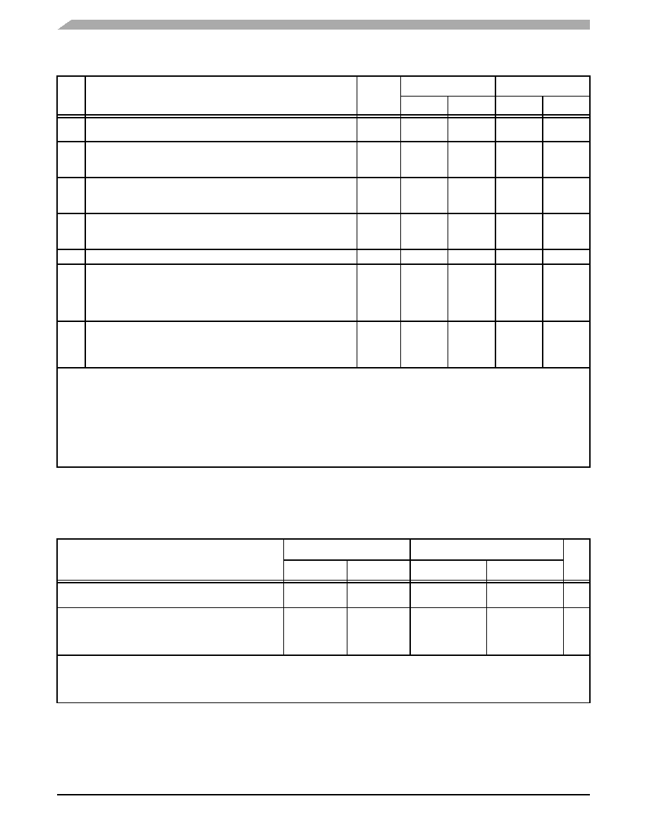
2.5.3
Phase Lock Loop (PLL) Characteristics
Table 2-5.
Clock Operation
No.
Characteristics
Symbol
80 MHz
100 MHz
Min
Max
Min
Max
1
Frequency of EXTAL (EXTAL Pin Frequency)
The rise and fall time of this external clock should be 3 ns maximum.
Ef
0
80.0 MHz
0
100.0 MHz
2
EXTAL input high1, 2
With PLL disabled (46.7%–53.3% duty cycle6)
With PLL enabled (42.5%–57.5% duty cycle6)
ETH
5.84 ns
5.31 ns
∞
157.0
μs
4.67 ns
4.25 ns
∞
157.0
μs
3
EXTAL input low1, 2
With PLL disabled (46.7%–53.3% duty cycle6)
With PLL enabled (42.5%–57.5% duty cycle6)
ETL
5.84 ns
5.31 ns
∞
157.0
μs
4.67 ns
4.25 ns
∞
157.0
μs
4
EXTAL cycle time2
With PLL disabled
With PLL enabled
ETC
12.50 ns
∞
273.1
μs
10.00 ns
∞
273.1
μs
5
CLKOUT change from EXTAL fall with PLL disabled
4.3 ns
11.0 ns
4.3 ns
11.0 ns
6
a. CLKOUT rising edge from EXTAL rising edge with PLL enabled (MF
= 1 or 2 or 4, PDF = 1, Ef > 15 MHz)3,5
b. CLKOUT falling edge from EXTAL falling edge with PLL enabled (MF
≤ 4, PDF ≠ 1, Ef / PDF > 15 MHz)3,5
0.0 ns
1.8 ns
0.0 ns
1.8 ns
7
Instruction cycle time = ICYC = TC
4
(see Table 2-4) (46.7%–53.3% duty cycle)
With PLL disabled
With PLL enabled
ICYC
25.0 ns
12.50 ns
∞
8.53
μs
20.0 ns
10.00 ns
∞
8.53
μs
Notes:
1.
Measured at 50 percent of the input transition
2.
The maximum value for PLL enabled is given for minimum VCO frequency (see Table 2-6) and maximum MF.
3.
Periodically sampled and not 100 percent tested
4.
The maximum value for PLL enabled is given for minimum VCO frequency and maximum DF.
5.
The skew is not guaranteed for any other MF value.
6.
The indicated duty cycle is for the specified maximum frequency for which a part is rated. The minimum clock high or low time
required for correction operation, however, remains the same at lower operating frequencies; therefore, when a lower clock
frequency is used, the signal symmetry may vary from the specified duty cycle as long as the minimum high time and low time
requirements are met.
Table 2-6.
PLL Characteristics
Characteristics
80 MHz
100 MHz
Unit
Min
Max
Min
Max
Voltage Controlled Oscillator (VCO) frequency when PLL
enabled (MF
× Ef × 2/PDF)
30
160
30
200
MHz
PLL external capacitor (PCAP pin to VCCP) (CPCAP
)
@ MF
≤ 4
@ MF > 4
(MF
× 580)
100
MF
× 830
(MF
× 780)
140
MF
× 1470
(MF
× 580) 100
MF
× 830
(MF
× 780) 140
MF
× 1470
pF
Note:
CPCAP is the value of the PLL capacitor (connected between the PCAP pin and VCCP). The recommended value in pF for CPCAP
can be computed from one of the following equations:
(680
× MF) – 120, for MF ≤ 4, or
1100
× MF, for MF > 4.
相关PDF资料 |
PDF描述 |
|---|---|
| DSP56303VL100B1 | IC DSP 24BIT 100MHZ 196-BGA |
| DSP56311VF150B1 | IC DSP 24BIT 150MHZ 196-BGA |
| DSP56321VF200R2 | IC DSP 24BIT 200MHZ 196-BGA |
| DSP56852VFE | IC DSP 16BIT 120MHZ 81-MAPBGA |
| DSP56854FGE | IC DSP 16BIT 120MHZ 128-LQFP |
相关代理商/技术参数 |
参数描述 |
|---|---|
| DSP56301VF80 | 功能描述:数字信号处理器和控制器 - DSP, DSC MAP DSP RoHS:否 制造商:Microchip Technology 核心:dsPIC 数据总线宽度:16 bit 程序存储器大小:16 KB 数据 RAM 大小:2 KB 最大时钟频率:40 MHz 可编程输入/输出端数量:35 定时器数量:3 设备每秒兆指令数:50 MIPs 工作电源电压:3.3 V 最大工作温度:+ 85 C 封装 / 箱体:TQFP-44 安装风格:SMD/SMT |
| DSP56301VF80B1 | 功能描述:数字信号处理器和控制器 - DSP, DSC DSP56301VF80B1 RoHS:否 制造商:Microchip Technology 核心:dsPIC 数据总线宽度:16 bit 程序存储器大小:16 KB 数据 RAM 大小:2 KB 最大时钟频率:40 MHz 可编程输入/输出端数量:35 定时器数量:3 设备每秒兆指令数:50 MIPs 工作电源电压:3.3 V 最大工作温度:+ 85 C 封装 / 箱体:TQFP-44 安装风格:SMD/SMT |
| DSP56301VL100 | 制造商:FREESCALE 制造商全称:Freescale Semiconductor, Inc 功能描述:24-Bit Digital Signal Processor |
| DSP56301VL80 | 制造商:FREESCALE 制造商全称:Freescale Semiconductor, Inc 功能描述:24-Bit Digital Signal Processor |
| DSP56302 | 制造商:MOTOROLA 制造商全称:Motorola, Inc 功能描述:DSP56301 Digital Signal Processor |
发布紧急采购,3分钟左右您将得到回复。