- 您现在的位置:买卖IC网 > PDF目录377488 > IDT88P8344BHGI (INTEGRATED DEVICE TECHNOLOGY INC) SPI EXCHANGE 4 x SPI-3 TO SPI-4 Issue 1.0 PDF资料下载
参数资料
| 型号: | IDT88P8344BHGI |
| 厂商: | INTEGRATED DEVICE TECHNOLOGY INC |
| 元件分类: | 微控制器/微处理器 |
| 英文描述: | SPI EXCHANGE 4 x SPI-3 TO SPI-4 Issue 1.0 |
| 中文描述: | SPECIALTY MICROPROCESSOR CIRCUIT, PBGA820 |
| 封装: | GREEN, PLASTIC, BGA-820 |
| 文件页数: | 77/98页 |
| 文件大小: | 601K |
| 代理商: | IDT88P8344BHGI |
第1页第2页第3页第4页第5页第6页第7页第8页第9页第10页第11页第12页第13页第14页第15页第16页第17页第18页第19页第20页第21页第22页第23页第24页第25页第26页第27页第28页第29页第30页第31页第32页第33页第34页第35页第36页第37页第38页第39页第40页第41页第42页第43页第44页第45页第46页第47页第48页第49页第50页第51页第52页第53页第54页第55页第56页第57页第58页第59页第60页第61页第62页第63页第64页第65页第66页第67页第68页第69页第70页第71页第72页第73页第74页第75页第76页当前第77页第78页第79页第80页第81页第82页第83页第84页第85页第86页第87页第88页第89页第90页第91页第92页第93页第94页第95页第96页第97页第98页
77
IDT88P8344 SPI EXCHANGE 4 x SPI-3 TO SPI-4
INDUSTRIAL TEMPERATURE RANGE
APRIL 10, 2006
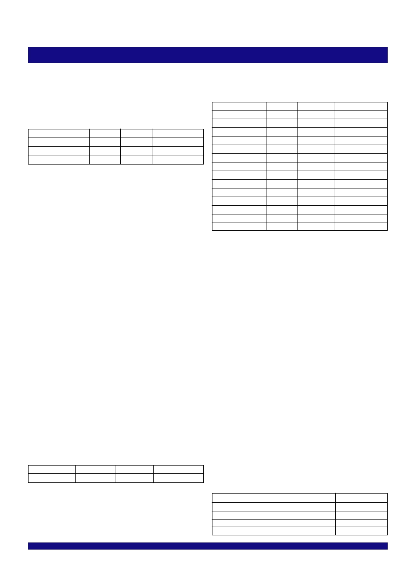
TABLE 122 - OCLK AND MCLK FREQUENCY
SELECT ENCODING
N_MCLK & N_OCLK[k] Frequency Selects
00
01
10
11
Frequency
pll_oclk / 4
pll_oclk / 6
pll_oclk / 8
pll_oclk / 10
TABLE 121 - CLOCK GENERATOR CONTROL
REGISTER (REGISTER_OFFSET 0x10)
Field
Bits
OCLK0_EN
0
N_OCLK0
2:1
Reserved
3
OCLK1_EN
4
N_OCLK1
6:5
Reserved
7
OCLK2_EN
8
N_OCLK2
10:9
Reserved
11
OCLK3_EN
12
N_OCLK3
14:13
Reserved
16:15
N_MCLK
18:17
Reserved
31:19
Length
1
2
1
1
2
1
1
2
1
1
2
2
2
13
Initial Value
0b01
0b11
0b0
0b1
0b11
0b0
0b1
0b11
0b0
0b1
0b11
0b0
0b11
0
9.4.10 Common module block base 0x0900 registers
PMON timebase control register (Block_base
0x0900 + Register_offset 0x00)
Field
Bits
0
1
2
Length
1
1
1
Initial Value
0b0
0b0
0b0
INTERNAL
TIMER
MANUAL
A single PMON timebase module is available in the IDT88P8344. The PMON
timebase module directs a timebase event to all PMON modules in the device.
The timebase period can be internally or externally generated. The selection
is made by the INTERNAL flag in the PMON update control register. A snapshot
of the counters is taken when the timebase expires and the counters are cleared.
The PMON update control register is at common module 0x8000 + Block_base
0x0900 + Register_offset 0x00 = 0x8900 and has read and write access.
TABLE 119 - PMON TIMEBASE CONTROL REGIS-
TER (REGISTER_OFFSET 0x00)
INTERNAL
mance monitoring. The internal timebase is either generated by the internal
processor or by a free running timer. The selection is made by the TIMER flag
in the PMON update control register. When the time interval expires, the
TIMEBASE pin is asserted for sixteen MCLK cycles. The timebase event is
captured by the timebase status in the support interrupt status register.
0= External timebase fromthe TIMEBASE pin is selected. The externally
generated timebase signal is applied to the TIMEBASE pin. A positive edge
detector generates the timebase event.
1=Internal timebase is selected. When the time interval expires, the TIMEBASE
pin is driven high for sixteen MCLK cycles.
Selects between internal or external timebases for perfor-
TIMER
Selects between the internal free-running timebase or a mcropro-
cessor-controlled write to generate the timebase event. The TIMER field is valid
only when the INTERNAL field is a logic one.
0=Selects the mcroprocessor generated timebase
1=Selects the internal free-running timebase
MANUAL
by a write access with a logical one to the MANUAL flag in the PMON Update
Control Register if the mcroprocessor timebase is selected. The MANUAL bit
is self-clearing. The MANUAL field is only valid if the TIMER field is a logic zero.
0=No operation
1=A timebase event is generated
The mcroprocessor generates an internal timebase event
Timebase register (Block_base 0x0900 +
Register_offset 0x01)
TABLE 120 - TIMEBASE REGISTER
(REGISTER_OFFSET 0x01)
Clock generator control register (Block_base
0x0900 + Register_offset 0x010)
The clock generator control register is at common module Block_base
0x0900 + Register_offset 0x010.
The clock generator provides four clock outputs on the OCLK[3:0] pins,
MCLK for internal use, and SPI-4 data and FIFO status channel egress clocks.
The OCLK[3:0] clock frequencies can be selected independently of each other.
OCLK[3:0] outputs can be used as SPI-3 clock sources. The OCLK[3:0] pins
are separately enabled by setting each associated enable flag in Table 121 -
Clock generator control register (Register_offset 0x10). When an OCLK[3:0]
output is not enabled, it is in a logic low state. MCLK is the internal processing
clock, and is always enabled. Refer to Table 122 - OCLK and MCLK frequency
select encoding, for selecting the frequencies of MCLK and OCLKs.
During either a hardware or a software reset, the OCLK[3:0] pins are all logic
low. Immediately following reset, all OCLK[3:0] outputs are active with the output
frequency defined by pll_oclk divided by the initial value in the Table 121 - Clock
generator control register (Block_base 0x0900 + Register_offset 0x10).
The clock generator control register at indirect address 0x8910 has read and
write access. The clock generator control register is used to set the frequency
of MCLK and the OCLK outputs, as well as to enable the OCLK outputs. Note
that divider values should be chosen so that OCLK[3:0] and MCLK are within
their specified operating range provided in Table 136, OCLK[3:0] clock outputs
and MCLK internal clock.
OCLK[k]_EN
Used for enabling the kth OCLK output
0=OCLK[k] is not enabled and OCLK[k] is at a logic zero
1=OCLK[k] is enabled and active
N_OCLK[k] [1:0]
Select the OCLK[k] frequency according to Table 122-
OCLK and MCLK frequency select encoding.
N_MCLK[k]
Select the MCLK frequency according to Table 122-OCLK
and MCLK frequency select encoding.
The timebase register is at Block_base 0x0900 + Register_offset 0x01 and
has read and write access.
The timebase period for free-running timers is configured by the PERIOD field
in the timebase register. The PERIOD field specifies the number of MCLK clock
cycles required for a single event. The PERIOD field is only valid if both the
INTERNAL and TIMER fields are a logic one.
Field
PERIOD
Bits
26:0
Length
27
Initial Value
0x4A2 8600
相关PDF资料 |
PDF描述 |
|---|---|
| IDTAMB0480 | ADVANCED MEMORY BUFFER FOR FULLY BUFFERED DIMM MODULES |
| IDTCSP2510DPGI | 3.3V PHASE-LOCK LOOP CLOCK DRIVER ZERO DELAY BUFFER |
| IDTCSP2510DPG | SENSOR OPTICAL SLOTTED 1.0MM |
| IDTCSP2510D | 3.3V PHASE-LOCK LOOP CLOCK DRIVER ZERO DELAY BUFFER |
| IDTCSPT857CNL | 2.5V - 2.6V PHASE LOCKED LOOP DIFFERENTIAL 1:10 SDRAM CLOCK DRIVER |
相关代理商/技术参数 |
参数描述 |
|---|---|
| IDT88P8344BHI | 功能描述:IC SPI3-SPI4 EXCHANGE 820-PBGA RoHS:否 类别:集成电路 (IC) >> 专用 IC 系列:* 产品培训模块:Lead (SnPb) Finish for COTS Obsolescence Mitigation Program 标准包装:1 系列:- 类型:调帧器 应用:数据传输 安装类型:表面贴装 封装/外壳:400-BBGA 供应商设备封装:400-PBGA(27x27) 包装:散装 |
| IDT89H10T4BG2ZBBC | 制造商:Integrated Device Technology Inc 功能描述:IC PCI SW 10LANE 4PORT 324BGA |
| IDT89H10T4BG2ZBBC8 | 制造商:Integrated Device Technology Inc 功能描述:IC PCI SW 10LANE 4PORT 324BGA |
| IDT89H10T4BG2ZBBCG | 功能描述:IC PCI SW 10LANE 4PORT 324BGA RoHS:是 类别:集成电路 (IC) >> 专用 IC 系列:PRECISE™ 产品培训模块:Lead (SnPb) Finish for COTS Obsolescence Mitigation Program 标准包装:1 系列:- 类型:调帧器 应用:数据传输 安装类型:表面贴装 封装/外壳:400-BBGA 供应商设备封装:400-PBGA(27x27) 包装:散装 |
| IDT89H10T4BG2ZBBCG8 | 制造商:Integrated Device Technology Inc 功能描述:IC PCI SW 10LANE 4PORT 324BGA |
发布紧急采购,3分钟左右您将得到回复。