- 您现在的位置:买卖IC网 > PDF目录69013 > M37274MA-XXXSP 8-BIT, MROM, MICROCONTROLLER, PDIP52 PDF资料下载
参数资料
| 型号: | M37274MA-XXXSP |
| 元件分类: | 微控制器/微处理器 |
| 英文描述: | 8-BIT, MROM, MICROCONTROLLER, PDIP52 |
| 封装: | 0.600 INCH, 1.778 MM PITCH, SHRINK, PLASTIC, DIP-52 |
| 文件页数: | 113/131页 |
| 文件大小: | 2049K |
| 代理商: | M37274MA-XXXSP |
第1页第2页第3页第4页第5页第6页第7页第8页第9页第10页第11页第12页第13页第14页第15页第16页第17页第18页第19页第20页第21页第22页第23页第24页第25页第26页第27页第28页第29页第30页第31页第32页第33页第34页第35页第36页第37页第38页第39页第40页第41页第42页第43页第44页第45页第46页第47页第48页第49页第50页第51页第52页第53页第54页第55页第56页第57页第58页第59页第60页第61页第62页第63页第64页第65页第66页第67页第68页第69页第70页第71页第72页第73页第74页第75页第76页第77页第78页第79页第80页第81页第82页第83页第84页第85页第86页第87页第88页第89页第90页第91页第92页第93页第94页第95页第96页第97页第98页第99页第100页第101页第102页第103页第104页第105页第106页第107页第108页第109页第110页第111页第112页当前第113页第114页第115页第116页第117页第118页第119页第120页第121页第122页第123页第124页第125页第126页第127页第128页第129页第130页第131页
82
SINGLE-CHIP 8-BIT CMOS MICROCOMPUTER with CLOSED CAPTION DECODER
and ON-SCREEN DISPLAY CONTROLLER
M37274MA-XXXSP
PRELIMINARY
Notice:
This
is not
a final
specification.
Some
paramentic
limits
are
subject
to change.
MITSUBISHI MICROCOMPUTERS
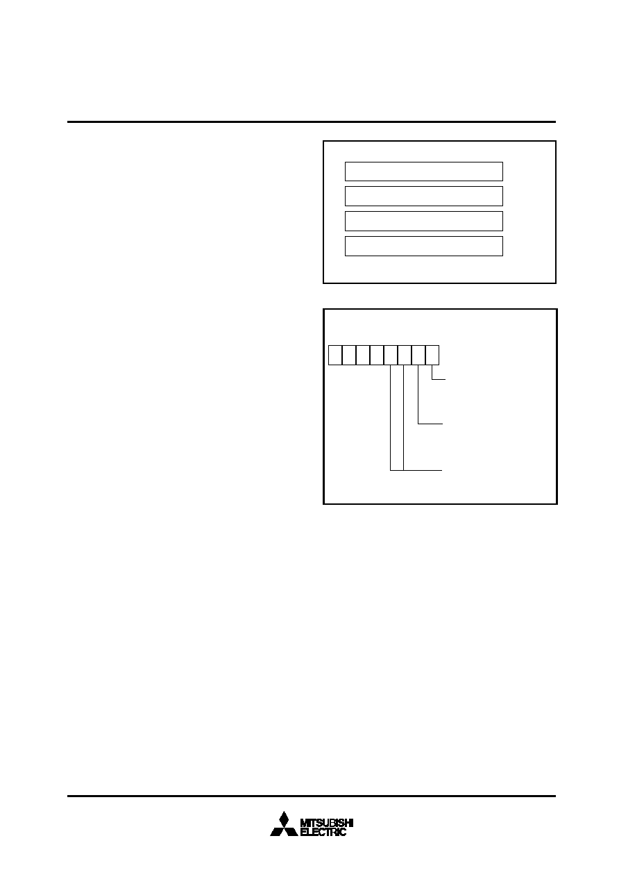
Fig. 92. ROM Correction Enable Register
Fig. 91. ROM Correction Address Registers
ROM CORRECTION FUNCTION
This can correct program data in ROM. Up to 2 addresses (2 blocks)
can be corrected, a program for correction is stored in the ROM cor-
rection memory in RAM. The ROM memory for correction is 32 bytes
! 2 blocks.
Block 1 : addresses 02C016 to 02DF16
Block 2 : addresses 02E016 to 02FF16
Set the address of the ROM data to be corrected into the ROM cor-
rection address register. When the value of the counter matches the
ROM data address in the ROM correction address, the main pro-
gram branches to the correction program stored in the ROM memory
for correction. To return from the correction program to the main pro-
gram, the op code and operand of the JMP instruction (total of 3
bytes) are necessary at the end of the correction program. When the
blocks 1 and 2 are used in series, the above instruction is not needed
at the end of the block 1.
The ROM correction function is controlled by the ROM correction
enable register.
Notes 1 : Specify the first address (op code address) of each
instruction as the ROM correction address.
2 : Use the JMP instruction (total of 3 bytes) to return from
the main program to the correction program.
3 : Do not set the same ROM correction address to blocks
1 and 2.
024216
ROM correction address 1 (high-order)
024316
ROM correction address 1 (low-order)
024416
ROM correction address 2 (high-order)
024516
ROM correction address 2 (low-order)
0
7
Fix these bits to “ 0.”
ROM correction enable register
(RCR : address 024616)
0
0 : Disabled
1 : Enabled
0 : Disabled
1 : Enabled
Block 1 enable bit
Block 2 enable bit
相关PDF资料 |
PDF描述 |
|---|---|
| M37373M8-XXXSP | 8-BIT, MROM, 8 MHz, MICROCONTROLLER, PDIP52 |
| M37409M2-XXXFP | 8-BIT, MROM, 10 MHz, MICROCONTROLLER, PQFP56 |
| M37413E6HXXXFP | 8-BIT, OTPROM, 8 MHz, MICROCONTROLLER, PQFP80 |
| M37413M4-XXXFP | 8-BIT, MROM, 8 MHz, MICROCONTROLLER, PQFP80 |
| M37420M4-XXXSP | 8-BIT, MROM, 8 MHz, MICROCONTROLLER, PDIP52 |
相关代理商/技术参数 |
参数描述 |
|---|---|
| M37276MF248SP | 制造商:MITSUBISHI 功能描述:* |
| M37276MF2575P | 制造商:MITSUBISHI 功能描述:* |
| M37276MF260SP | 制造商:MITSUBISHI 功能描述:* |
| M37276MF300SP | 制造商:MITSUBISHI 功能描述:* |
| M37276MF301SP | 制造商:MITSUBISHI 功能描述:* |
发布紧急采购,3分钟左右您将得到回复。