- 您现在的位置:买卖IC网 > PDF目录69013 > M37274MA-XXXSP 8-BIT, MROM, MICROCONTROLLER, PDIP52 PDF资料下载
参数资料
| 型号: | M37274MA-XXXSP |
| 元件分类: | 微控制器/微处理器 |
| 英文描述: | 8-BIT, MROM, MICROCONTROLLER, PDIP52 |
| 封装: | 0.600 INCH, 1.778 MM PITCH, SHRINK, PLASTIC, DIP-52 |
| 文件页数: | 71/131页 |
| 文件大小: | 2049K |
| 代理商: | M37274MA-XXXSP |
第1页第2页第3页第4页第5页第6页第7页第8页第9页第10页第11页第12页第13页第14页第15页第16页第17页第18页第19页第20页第21页第22页第23页第24页第25页第26页第27页第28页第29页第30页第31页第32页第33页第34页第35页第36页第37页第38页第39页第40页第41页第42页第43页第44页第45页第46页第47页第48页第49页第50页第51页第52页第53页第54页第55页第56页第57页第58页第59页第60页第61页第62页第63页第64页第65页第66页第67页第68页第69页第70页当前第71页第72页第73页第74页第75页第76页第77页第78页第79页第80页第81页第82页第83页第84页第85页第86页第87页第88页第89页第90页第91页第92页第93页第94页第95页第96页第97页第98页第99页第100页第101页第102页第103页第104页第105页第106页第107页第108页第109页第110页第111页第112页第113页第114页第115页第116页第117页第118页第119页第120页第121页第122页第123页第124页第125页第126页第127页第128页第129页第130页第131页
44
MITSUBISHI MICROCOMPUTERS
SINGLE-CHIP 8-BIT CMOS MICROCOMPUTER with CLOSED CAPTION DECODER
and ON-SCREEN DISPLAY CONTROLLER
M37274MA-XXXSP
PRELIMINARY
Notice:
This
is not
a final
specification.
Some
paramentic
limits
are
subject
to change.
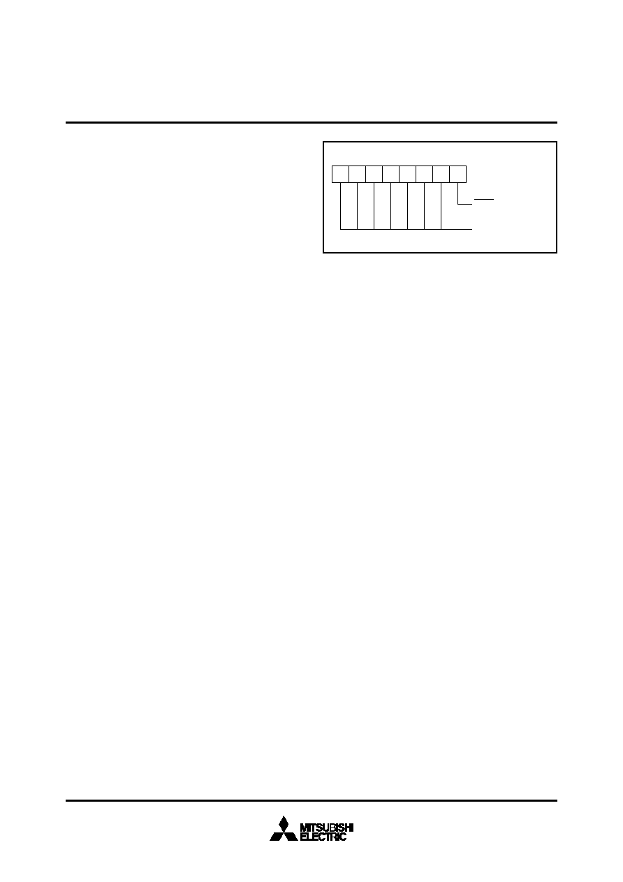
SAD6 SAD5 SAD4 SAD3 SAD2 SAD1 SAD0 RBW
Slave address
I2 C address register
(S0D: address 00F716)
Read/write bit
70
(1) I2C Data Shift Register
The I2C data shift register (S0 : address 00F616) is an 8-bit shift
register to store receive data and write transmit data.
When transmit data is written into this register, it is transferred to the
outside from bit 7 in synchronization with the SCL clock, and each
time one-bit data is output, the data of this register are shifted one bit
to the left. When data is received, it is input to this register from bit 0
in synchronization with the SCL clock, and each time one-bit data is
input, the data of this register are shifted one bit to the left.
The I2C data shift register is in a write enable status only when the
ESO bit of the I2C control register (address 00F916) is “1.” The bit
counter is reset by a write instruction to the I2C data shift register.
When both the ESO bit and the MST bit of the I2C status register
(address 00F816) are “1,” the SCL is output by a write instruction to
the I2C data shift register. Reading data from the I2C data shift regis-
ter is always enabled regardless of the ESO bit value.
Note: To write data into the I2C data shift register after setting the
MST bit to “0” (slave mode), keep an interval of 8 machine
cycles or more.
(2) I2C Address Register
The I2C address register (address 00F716) consists of a 7-bit slave
___
address and a read/write bit. In the addressing mode, the slave ad-
dress written in this register is compared with the address data to be
received immediately after the START condition are detected.
____
s Bit 0: Read/Write Bit (RBW)
Not used when comparing addresses, in the 7-bit addressing mode.
In the 10-bit addressing mode, the first address data to be received
is compared with the contents (SAD6 to SAD0 + RBW) of the I2C
address register.
The RBW bit is cleared to “0” automatically when the stop condition
is detected.
s Bits 1 to 7: Slave Address (SAD0–SAD6)
These bits store slave addresses. Regardless of the 7-bit address-
ing mode and the 10-bit addressing mode, the address data trans-
mitted from the master is compared with the contents of these bits.
(3) I2C Clock Control Register
The I2C clock control register (address 00FA16) is used to set ACK
control, SCL mode and SCL frequency.
s Bits 0 to 4: SCL Frequency Control Bits (CCR0–CCR4)
These bits control the SCL frequency. Refer to Table 7.
s Bit 5: SCL Mode Specification Bit (FAST MODE)
This bit specifies the SCL mode. When this bit is set to “0,” the stan-
dard clock mode is set. When the bit is set to “1,” the high-speed
clock mode is set.
s Bit 6: ACK Bit (ACK BIT)
This bit sets the SDA status when an ACK clockV is generated. When
this bit is set to “0,” the ACK return mode is set and SDA goes to
LOW at the occurrence of an ACK clock. When the bit is set to “1,”
the ACK non-return mode is set. The SDA is held in the HIGH status
at the occurrence of an ACK clock.
However, when the slave address matches the address data in the
reception of address data at ACK BIT = “0,” the SDA is automatically
made LOW (ACK is returned). If there is a mismatch between the
slave address and the address data, the SDA is automatically made
HIGH (ACK is not returned).
VACK clock: Clock for acknowledgement
s Bit 7: ACK Clock Bit (ACK)
This bit specifies a mode of acknowledgment which is an acknowl-
edgment response of data transmission. When this bit is set to “0,”
the no ACK clock mode is set. In this case, no ACK clock occurs
after data transmission. When the bit is set to “1,” the ACK clock
mode is set and the master generates an ACK clock upon comple-
tion of each 1-byte data transmission.The device for transmitting
address data and control data releases the SDA at the occurrence of
an ACK clock (make SDA HIGH) and receives the ACK bit gener-
ated by the data receiving device.
Note: Do not write data into the I2C clock control register during
transmission. If data is written during transmission, the I2C
clock generator is reset, so that data cannot be transmitted
normally.
Fig. 43. I2C Address Register
相关PDF资料 |
PDF描述 |
|---|---|
| M37373M8-XXXSP | 8-BIT, MROM, 8 MHz, MICROCONTROLLER, PDIP52 |
| M37409M2-XXXFP | 8-BIT, MROM, 10 MHz, MICROCONTROLLER, PQFP56 |
| M37413E6HXXXFP | 8-BIT, OTPROM, 8 MHz, MICROCONTROLLER, PQFP80 |
| M37413M4-XXXFP | 8-BIT, MROM, 8 MHz, MICROCONTROLLER, PQFP80 |
| M37420M4-XXXSP | 8-BIT, MROM, 8 MHz, MICROCONTROLLER, PDIP52 |
相关代理商/技术参数 |
参数描述 |
|---|---|
| M37276MF248SP | 制造商:MITSUBISHI 功能描述:* |
| M37276MF2575P | 制造商:MITSUBISHI 功能描述:* |
| M37276MF260SP | 制造商:MITSUBISHI 功能描述:* |
| M37276MF300SP | 制造商:MITSUBISHI 功能描述:* |
| M37276MF301SP | 制造商:MITSUBISHI 功能描述:* |
发布紧急采购,3分钟左右您将得到回复。