- 您现在的位置:买卖IC网 > PDF目录69013 > M37274MA-XXXSP 8-BIT, MROM, MICROCONTROLLER, PDIP52 PDF资料下载
参数资料
| 型号: | M37274MA-XXXSP |
| 元件分类: | 微控制器/微处理器 |
| 英文描述: | 8-BIT, MROM, MICROCONTROLLER, PDIP52 |
| 封装: | 0.600 INCH, 1.778 MM PITCH, SHRINK, PLASTIC, DIP-52 |
| 文件页数: | 99/131页 |
| 文件大小: | 2049K |
| 代理商: | M37274MA-XXXSP |
第1页第2页第3页第4页第5页第6页第7页第8页第9页第10页第11页第12页第13页第14页第15页第16页第17页第18页第19页第20页第21页第22页第23页第24页第25页第26页第27页第28页第29页第30页第31页第32页第33页第34页第35页第36页第37页第38页第39页第40页第41页第42页第43页第44页第45页第46页第47页第48页第49页第50页第51页第52页第53页第54页第55页第56页第57页第58页第59页第60页第61页第62页第63页第64页第65页第66页第67页第68页第69页第70页第71页第72页第73页第74页第75页第76页第77页第78页第79页第80页第81页第82页第83页第84页第85页第86页第87页第88页第89页第90页第91页第92页第93页第94页第95页第96页第97页第98页当前第99页第100页第101页第102页第103页第104页第105页第106页第107页第108页第109页第110页第111页第112页第113页第114页第115页第116页第117页第118页第119页第120页第121页第122页第123页第124页第125页第126页第127页第128页第129页第130页第131页
7
SINGLE-CHIP 8-BIT CMOS MICROCOMPUTER with CLOSED CAPTION DECODER
and ON-SCREEN DISPLAY CONTROLLER
M37274MA-XXXSP
PRELIMINARY
Notice:
This
is not
a final
specification.
Some
paramentic
limits
are
subject
to change.
MITSUBISHI MICROCOMPUTERS
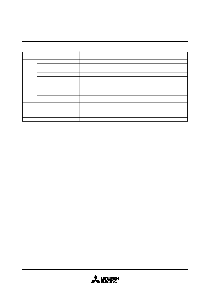
Ports P63 and P64 are 2-bit input port.
Pin P63 is also used as OSD clock input pin OSC1.
Pin P64 is also used as OSD clock output pin OSC2. The output structure is CMOS output.
Pin P64 is also used as sub-clock output pin XCOUT. The output structure is CMOS output.
Pin P63 is also used as sub-clock input pin XCIN.
Ports P70–P72 are 3-bit input port.
Pins P70, P71 are also used as data slicer input pins CVIN, VHOLD respectively. When
using data slicer, input composite video signal through a capacitor. Connect a capacitor
between VHOLD and VSS.
Pins P72 pin is also used as input/output pin for data slicer RVCO. When using data slicer,
connect a resistor between RVCO and VSS.
When using data slicer, connect a filter using of a capacitor and a resistor between HLF
and VSS.
This is a horizontal synchronous signal input for OSD.
This is a vertical synchronous signal input for OSD.
PIN DESCRIPTION (continued)
Note : As shown in the memory map (Figure 5), port P0 is accessed as a memory at address 00C016 of zero page. Port P0 has the port P0
direction register (address 00C116 of zero page) which can be used to program each bit as an input (“0”) or an output (“1”). The pins
programmed as “1” in the direction register are output pins. When pins are programmed as “0,” they are input pins. When pins are
programmed as output pins, the output data are written into the port latch and then output. When data is read from the output pins, the
output pin level is not read but the data of the port latch is read. This allows a previously-output value to be read correctly even if the
output “L” voltage has risen, for example, because a light emitting diode was directly driven. The input pins float, so the values of the pins
can be read. When data is written into the input pin, it is written only into the port latch, while the pin remains in the floating state.
Pin
Name
Functions
Input/
Output
Analog input
Input
This is an analog input pin AD6.
I/O
Input/output for
data slicer
P63/OSC1/
XCIN,
P64/OSC2/
XCOUT
P70/CVIN,
P71/VHOLD,
P72/RVCO
HLF/AD6
HSYNC
VSYNC
Input port
Clock input for OSD
Clock output for OSD
Sub-clock output
Sub-clock input
Input port P7
Input for data slicer
HSYNC input
VSYNC input
Input
Output
Input
相关PDF资料 |
PDF描述 |
|---|---|
| M37373M8-XXXSP | 8-BIT, MROM, 8 MHz, MICROCONTROLLER, PDIP52 |
| M37409M2-XXXFP | 8-BIT, MROM, 10 MHz, MICROCONTROLLER, PQFP56 |
| M37413E6HXXXFP | 8-BIT, OTPROM, 8 MHz, MICROCONTROLLER, PQFP80 |
| M37413M4-XXXFP | 8-BIT, MROM, 8 MHz, MICROCONTROLLER, PQFP80 |
| M37420M4-XXXSP | 8-BIT, MROM, 8 MHz, MICROCONTROLLER, PDIP52 |
相关代理商/技术参数 |
参数描述 |
|---|---|
| M37276MF248SP | 制造商:MITSUBISHI 功能描述:* |
| M37276MF2575P | 制造商:MITSUBISHI 功能描述:* |
| M37276MF260SP | 制造商:MITSUBISHI 功能描述:* |
| M37276MF300SP | 制造商:MITSUBISHI 功能描述:* |
| M37276MF301SP | 制造商:MITSUBISHI 功能描述:* |
发布紧急采购,3分钟左右您将得到回复。