- 您现在的位置:买卖IC网 > PDF目录299522 > MT18HTF12872G-40EC2 128M X 72 DDR DRAM MODULE, 0.6 ns, DMA240 PDF资料下载
参数资料
| 型号: | MT18HTF12872G-40EC2 |
| 元件分类: | DRAM |
| 英文描述: | 128M X 72 DDR DRAM MODULE, 0.6 ns, DMA240 |
| 封装: | DIMM-240 |
| 文件页数: | 19/36页 |
| 文件大小: | 672K |
| 代理商: | MT18HTF12872G-40EC2 |
第1页第2页第3页第4页第5页第6页第7页第8页第9页第10页第11页第12页第13页第14页第15页第16页第17页第18页当前第19页第20页第21页第22页第23页第24页第25页第26页第27页第28页第29页第30页第31页第32页第33页第34页第35页第36页
512MB, 1GB, 2GB (x72, REGISTERED)
PC2-3200, PC2-4300, 240-Pin DDR2 SDRAM DIMM
09005aef80e5e626
Micron Technology, Inc., reserves the right to change products or specifications without notice.
HTF18C64_128_256x72G_A.fm - Rev. A 9/03 EN
26
2003 Micron Technology. Inc.
Notes
1. All voltages referenced to VSS.
2. Tests for AC timing, IDD, and electrical AC and DC
characteristics may be conducted at nominal ref-
erence/supply voltage levels, but the related spec-
ifications and device operation are guaranteed for
the full voltage range specified.
3. Outputs measured with equivalent load:
4. AC timing and IDD tests may use a VIL-to-VIH swing
of up to 1.0V in the test environment and parame-
ter specifications are guaranteed for the specified
AC input levels under normal use conditions. The
minimum slew rate for the input signals used to
test the device is 1.0V/ns for signals in the range
between VIL (AC) and VIH (AC).
5. The AC and DC input level specifications are as
defined in the SSTL_18 standard (i.e., the receiver
will effectively switch as a result of the signal
crossing the AC input level and will remain in that
state as long as the signal does not ring back
above [below] the DC input LOW [HIGH] level).
6. Command/Address minimum input slew rate =
1.0V/ns and is referenced to the crosspoint of CK/
CK#. tIS timing is referenced to Vih(ac) for a rising
signal and VIL (AC) for a falling signal . tIH timing
is referenced to VIH (DC) for a rising signal and VIL
(DC) for a falling signal. Derating values for Com-
mand/Address input signal slew rates < 1.0V/ns
are TBD.
7. Data minimum input slew rate = 1.0V/ns and is
referenced to the crosspoint of DQS/DQS# if dif-
ferential strobe feature is enabled. tDS timing is
referenced to VIH (AC) for a rising signal and VIL
(AC) for a falling signal. tDH timing is referenced
to VIH (DC) for a rising signal and VIL (DC) for a
falling signal. Derating values for Data input sig-
nal slew rates < 1.0V/ns are TBD.
8. tHZ and tLZ transitions occur in the same access
time windows as valid data transitions.
These
parameters are not referenced to a specific voltage
level, but specify when the device output is no
longer driving (tHZ) or begins driving (tLZ).
9. This maximum value is derived from the refer-
enced test load. tHZ (MAX) will prevail over
tDQSCK (MAX) + tRPST (MAX) condition.
10. tLZ (MIN) will prevail over a tDQSCK (MIN) +
tRPRE (MAX) condition.
11. The intent of the Don’t Care state after completion
of the postamble is the DQS-driven signal should
either be high, low or high-Z and that any signal
transition within the input switching region must
follow valid input requirements. That is if DQS
transitions high [above VIH DC (MIN)] then it
must not transition low (below VIH DC) prior to
tDQSH(min).
12. This is not a device limit. The device will operate
with a negative value, but system performance
could be degraded due to bus turnaround.
13. It is recommended that DQS be valid (HIGH or
LOW) on or before the WRITE command. The
case shown (DQS going from High-Z to logic
LOW) applies when no WRITEs were previously in
progress on the bus. If a previous WRITE was in
progress, DQS could be HIGH during this time,
depending on tDQSS.
14. The refresh period is 64ms. This equates to an
average refresh rate of 7.8125s. However, an
REFRESH command must be asserted at least
once every 70.3s or tRFC (MAX); issuing more
than eight REFRESH commands back-to-back at
tRFC (MIN) is not allowed.
15. Each byte lane has a corresponding DQS.
16. CK and CK# input slew rate must be
1 V/ns ( 2
V/ns if measured differentially).
17. The data valid window is derived by achieving
other specifications: tHP, (tCK/2), tDQSQ, and tQH
(tQH = tHP - tQHS). The data valid window derates
in direct proportion to the clock duty cycle and a
practicle data valid window can be derived.
18. tJIT specification is currently TBD.
19. MIN( tCL, tCH) refers to the smaller of the actual
clock low time and the actual clock high time as
provided to the device (i.e. this value can be
greater than the minimum specification limits for
tCL and tCH). For example, tCL and tCH are = 50
percent of the period, less the half period jitter
[tJIT(HP)] of the clock source, and less the half
period jitter due to cross talk [tJIT(cross talk)] into
the clock traces.
20. tHP (MIN) is the lesser of tCL minimum and tCH
minimum actually applied to the device CK and
CK# inputs.
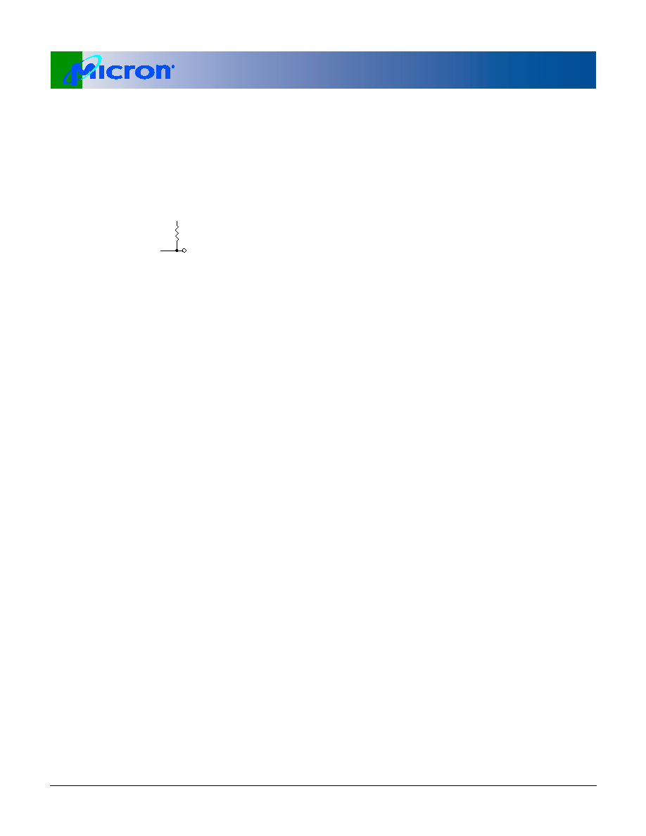
Output
(VOUT)
Reference
Point
25
VTT = VDDQ/2
相关PDF资料 |
PDF描述 |
|---|---|
| MT18HVF6472PY-53EXX | 64M X 72 DDR DRAM MODULE, 0.5 ns, DMA240 |
| MT28C128532W30DFW-F706P85BBWT | SPECIALTY MEMORY CIRCUIT, PBGA77 |
| MT28C128564W30DBW-F706P85KBTWT | SPECIALTY MEMORY CIRCUIT, PBGA77 |
| MT28C128532W30EFW-F705-P856KBBWT | SPECIALTY MEMORY CIRCUIT, PBGA77 |
| MT28C128532W18EFW-F605-P706BTWT | SPECIALTY MEMORY CIRCUIT, PBGA77 |
相关代理商/技术参数 |
参数描述 |
|---|---|
| MT18HTF12872JDY-667F1D4 | 制造商:Micron Technology Inc 功能描述:1GB 128MX72 DDR2 SDRAM MODULE COMMERCIAL PBF DIMM 1.8V FULLY - Bulk |
| MT18HTF12872M2DY-667F1B4 | 制造商:Micron Technology Inc 功能描述:1GB 128MX72 DDR2 SDRAM MODULE PBF DIMM 1.8V FULLY BUFFERED - Trays |
| MT18HTF12872M2DY-667F1B5 | 制造商:Micron Technology Inc 功能描述:1GB 128MX72 DDR2 SDRAM MODULE CUSTOM 1.8V FULLY BUFFERED - Trays |
| MT18HTF12872M2Y-53EF1 | 制造商:Micron Technology Inc 功能描述:1GB 128MX72 DDR2 SDRAM MODULE COMMERCIAL CUSTOM 1.8V REGISTE - Bulk |
| MT18HTF12872M3Y-53EF1 | 制造商:Micron Technology Inc 功能描述:1GB 128MX72 DDR2 SDRAM MODULE COMMERCIAL CUSTOM 1.8V REGISTE - Bulk |
发布紧急采购,3分钟左右您将得到回复。