- 您现在的位置:买卖IC网 > PDF目录299522 > MT18HTF12872G-40EC2 128M X 72 DDR DRAM MODULE, 0.6 ns, DMA240 PDF资料下载
参数资料
| 型号: | MT18HTF12872G-40EC2 |
| 元件分类: | DRAM |
| 英文描述: | 128M X 72 DDR DRAM MODULE, 0.6 ns, DMA240 |
| 封装: | DIMM-240 |
| 文件页数: | 5/36页 |
| 文件大小: | 672K |
| 代理商: | MT18HTF12872G-40EC2 |
第1页第2页第3页第4页当前第5页第6页第7页第8页第9页第10页第11页第12页第13页第14页第15页第16页第17页第18页第19页第20页第21页第22页第23页第24页第25页第26页第27页第28页第29页第30页第31页第32页第33页第34页第35页第36页
512MB, 1GB, 2GB (x72, REGISTERED)
PC2-3200, PC2-4300, 240-Pin DDR2 SDRAM DIMM
09005aef80e5e626
Micron Technology, Inc., reserves the right to change products or specifications without notice.
HTF18C64_128_256x72G_A.fm - Rev. A 9/03 EN
13
2003 Micron Technology. Inc.
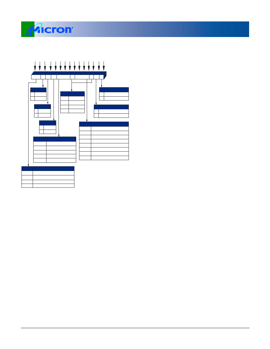
Figure 7: Extended Mode Register
Definition
NOTE:
1GB and 2GB extended mode registers TBD.
On Die Termination (ODT)
ODT effective resistance RTT (EFF) is defined by bits
E2 and E6 of the EMR as shown in Figure 7. The ODT
feature is designed to improve signal integrity of the
memory channel by allowing the DDR2 SDRAM con-
troller to independently turn on/off ODT for any or all
devices. RTT effective resistance values of 75
W and
150
W are selectable and apply to each DQ and DQS/
DQS# signal.
Bits (E6, E2) determine what ODT resistance is
enabled by turning on/off ‘sw1’ or ‘sw2’. The ODT
effective resistance value is selected by enabling switch
‘sw1,’ which enables all ‘R1’ values that are 150
W each,
enabling an effective resistance of 75
W (RTT (EFF1) =
‘R1’ / 2). Similarly, if ‘sw2’ is enabled, all ‘R2’ values
that are 300
W each, enable an effective ODT resistance
of 150
W (RTT (EFF2) = ‘R2’/2). Reserved states should
not be used, as unknown operation or incompatibility
with future versions may result.
The ODT control pin is used to determine when
RTT(EFF) is turned on and off, assuming ODT has been
enabled via bits E2 and E6 of the EMR. The ODT fea-
ture and ODT input pin are only used during active,
active power-down (both fast-exit and slow-exit
modes), and precharge power-down modes of opera-
tion. If SELF REFRESH operation is used, RTT (EFF)
should always be disabled and the ODT input pin is
disabled by the DDR2 SDRAM. During power-up and
initialization of the DDR2 SDRAM, ODT should be dis-
abled until the EMR command is issued to enable the
ODT feature, at which point the ODT pin will deter-
mine the RTT (EFF) value.
Off-Chip Driver (OCD) Impedance
Calibration
The DDR2 SDRAM output off-chip (OCD) driver
impedance calibration operation is defined by bits E7–
E9. OCD is intended to allow the system to calibrate
and match pull-up to pull-down impedance to 18
W
nominal. OCD is not indended to allow a wide range of
impedance calibration outside of the 18
W nominal
driver impedance.
Posted CAS Additive Latency (AL)
Posted CAS additive latency (AL) is supported to
make the command and data bus efficient for sustain-
able bandwidths in DDR2 SDRAM. Bits E3–E5 define
the value of AL as shown in Figure 7. Bits E3–E5 allow
the user to program the DDR2 SDRAM with a CAS#
Additive latency of 0, 1, 2, 3, or 4 clocks. Reserved states
should not be used as unknown operation or incom-
patibility with future versions may result.
In this operation, the DDR2 SDRAM allows a READ
or WRITE command to be issued prior to tRCD (MIN)
with the requirement that AL
tRCD(MIN). A typical
application using this feature would set AL = tRCD
(MIN) - 1 x tCK. The READ or WRITE command is held
for the time of the additive latency (AL) before it is
issued internally to the DDR2 SDRAM device. READ
Latency (RL) is controlled by the sum of the Posted
CAS additive latency (AL) and CAS Latency (CL); RL =
AL + CL. Write latency (WL) is equal to READ latency
minus one clock; WL = AL + CL - 1 x tCK. An example
of a READ latency is shown in Figure 8. An example of
a WRITE latency is shown in Figure 9.
DLL
Posted CAS# RTT
out
A9
A7 A6 A5 A4 A3
A8
A2
A1 A0
Extended Mode
Register (Ex)
Address Bus
97
6
5
4
3
82
1
0
A10
A12 A11
BA0
BA1
10
11
12
13
0
1
Output Drive Strength
100%
60%
E1
Posted CAS# Additive Latency (AL)
0
1
2
3
4
Reserved
E3
0
1
0
1
0
1
0
1
E4
0
1
0
1
E5
0
1
0
1
DLL Enable
Enable (Normal)
Disable (Test/Debug)
E0
14
0
1
RDQS Enable
No
Yes
E11
OCD Program
ODS
RTT
DQS#
0
1
DQS# Enable
Enable
Disable
E10
RDQS
RTT (nominal)
RTT Disabled
75 ohm
150 ohm
Reserved
E2
0
1
0
1
E6
0
1
OCD Operation
OCD calibration mode exit
Drive(1) pull-up
Drive(0) pull-down
OCD enter adjust mode
OCD calibration default
E7
0
1
0
1
E8
0
1
0
1
E9
0
1
0
1
Outputs
Enabled
Disabled
E12
0
1
0
1
Mode Register
Mode Register (MR)
Extended Mode Register (EMR)
Extended Mode Register (EMR2)
Extended Mode Register (EMR3)
M14
0
0
1
M13
EMR
相关PDF资料 |
PDF描述 |
|---|---|
| MT18HVF6472PY-53EXX | 64M X 72 DDR DRAM MODULE, 0.5 ns, DMA240 |
| MT28C128532W30DFW-F706P85BBWT | SPECIALTY MEMORY CIRCUIT, PBGA77 |
| MT28C128564W30DBW-F706P85KBTWT | SPECIALTY MEMORY CIRCUIT, PBGA77 |
| MT28C128532W30EFW-F705-P856KBBWT | SPECIALTY MEMORY CIRCUIT, PBGA77 |
| MT28C128532W18EFW-F605-P706BTWT | SPECIALTY MEMORY CIRCUIT, PBGA77 |
相关代理商/技术参数 |
参数描述 |
|---|---|
| MT18HTF12872JDY-667F1D4 | 制造商:Micron Technology Inc 功能描述:1GB 128MX72 DDR2 SDRAM MODULE COMMERCIAL PBF DIMM 1.8V FULLY - Bulk |
| MT18HTF12872M2DY-667F1B4 | 制造商:Micron Technology Inc 功能描述:1GB 128MX72 DDR2 SDRAM MODULE PBF DIMM 1.8V FULLY BUFFERED - Trays |
| MT18HTF12872M2DY-667F1B5 | 制造商:Micron Technology Inc 功能描述:1GB 128MX72 DDR2 SDRAM MODULE CUSTOM 1.8V FULLY BUFFERED - Trays |
| MT18HTF12872M2Y-53EF1 | 制造商:Micron Technology Inc 功能描述:1GB 128MX72 DDR2 SDRAM MODULE COMMERCIAL CUSTOM 1.8V REGISTE - Bulk |
| MT18HTF12872M3Y-53EF1 | 制造商:Micron Technology Inc 功能描述:1GB 128MX72 DDR2 SDRAM MODULE COMMERCIAL CUSTOM 1.8V REGISTE - Bulk |
发布紧急采购,3分钟左右您将得到回复。