- 您现在的位置:买卖IC网 > PDF目录4024 > MT42L192M32D3LE-3 IT:A (Micron Technology Inc)IC LPDDR2 SDRAM 8GBIT 168FBGA PDF资料下载
参数资料
| 型号: | MT42L192M32D3LE-3 IT:A |
| 厂商: | Micron Technology Inc |
| 文件页数: | 144/164页 |
| 文件大小: | 0K |
| 描述: | IC LPDDR2 SDRAM 8GBIT 168FBGA |
| 标准包装: | 1,000 |
| 格式 - 存储器: | RAM |
| 存储器类型: | 移动 LPDDR2 SDRAM |
| 存储容量: | 6G(192M x 32) |
| 速度: | 333MHz |
| 接口: | 并联 |
| 电源电压: | 1.14 V ~ 1.3 V |
| 工作温度: | -25°C ~ 85°C |
| 封装/外壳: | 168-VFBGA |
| 供应商设备封装: | 168-FBGA(12x12) |
| 包装: | 散装 |
第1页第2页第3页第4页第5页第6页第7页第8页第9页第10页第11页第12页第13页第14页第15页第16页第17页第18页第19页第20页第21页第22页第23页第24页第25页第26页第27页第28页第29页第30页第31页第32页第33页第34页第35页第36页第37页第38页第39页第40页第41页第42页第43页第44页第45页第46页第47页第48页第49页第50页第51页第52页第53页第54页第55页第56页第57页第58页第59页第60页第61页第62页第63页第64页第65页第66页第67页第68页第69页第70页第71页第72页第73页第74页第75页第76页第77页第78页第79页第80页第81页第82页第83页第84页第85页第86页第87页第88页第89页第90页第91页第92页第93页第94页第95页第96页第97页第98页第99页第100页第101页第102页第103页第104页第105页第106页第107页第108页第109页第110页第111页第112页第113页第114页第115页第116页第117页第118页第119页第120页第121页第122页第123页第124页第125页第126页第127页第128页第129页第130页第131页第132页第133页第134页第135页第136页第137页第138页第139页第140页第141页第142页第143页当前第144页第145页第146页第147页第148页第149页第150页第151页第152页第153页第154页第155页第156页第157页第158页第159页第160页第161页第162页第163页第164页
�� �
�
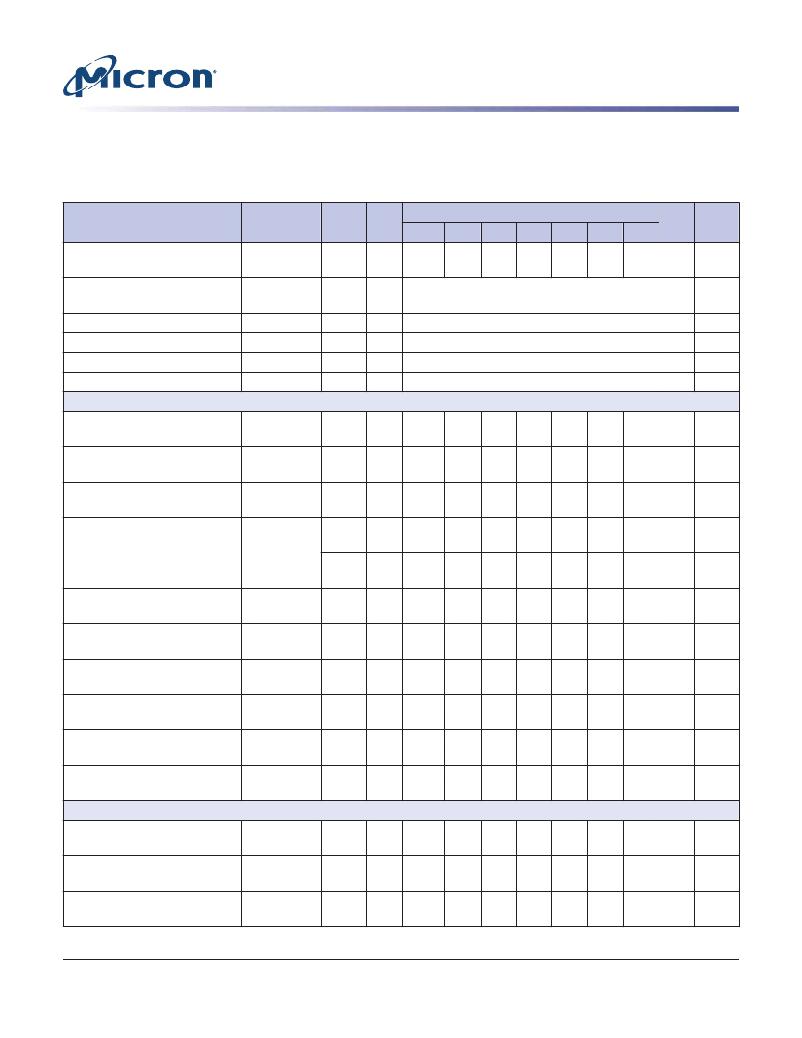
�2Gb:� x16,� x32� Mobile� LPDDR2� SDRAM� S4�
�AC� Timing�
�Table� 86:� AC� Timing� (Continued)�
�Notes� 1–2� apply� to� all� parameters� and� conditions.� AC� timing� parameters� must� satisfy� the� t� CK� minimum� conditions� (in� mul-�
�tiples� of� t� CK)� as� well� as� the� timing� specifications� when� values� for� both� are� indicated.�
�Min/M� t� CK�
�Data� Rate�
�Parameter�
�Symbol�
�ax�
�Min�
�1066�
�933�
�800�
�667�
�533�
�400�
�333�
�Unit� Notes�
�READ� preamble�
�t� RPRE�
�MIN�
�–�
�0.9�
�0.9�
�0.9�
�0.9�
�0.9�
�0.9�
�0.9�
�t� CK(a�
�7�
�vg)�
�READ� postamble�
�t� RPST�
�MIN�
�–�
�t� CL(abs)�
�-� 0.05�
�t� CK(a�
�8�
�vg)�
�DQS� Low-Z� from� clock�
�t� LZ(DQS)�
�MIN�
�–�
�t� DQSCK�
�(MIN)� -� 300�
�ps�
�DQ� Low-Z� from� clock�
�t� LZ(DQ)�
�MIN�
�–�
�t� DQSCK(MIN)�
�-� (1.4� �
�t� QHS(MAX))�
�ps�
�DQS� High-Z� from� clock�
�t� HZ(DQS)�
�MAX�
�–�
�t� DQSCK�
�(MAX)� -� 100�
�ps�
�DQ� High-Z� from� clock�
�t� HZ(DQ)�
�MAX�
�–�
�t� DQSCK(MAX)�
�+� (1.4� �
�t� DQSQ(MAX))�
�ps�
�WRITE�
�Parameters� 3�
�DQ� and� DM� input� hold� time�
�t� DH�
�MIN�
�–�
�210�
�235�
�270�
�350�
�430�
�480�
�600�
�ps�
�(V� REF� based)�
�DQ� and� DM� input� setup� time�
�t� DS�
�MIN�
�–�
�210�
�235�
�270�
�350�
�430�
�480�
�600�
�ps�
�(V� REF� based)�
�DQ� and� DM� input� pulse� width�
�t� DIPW�
�MIN�
�–�
�0.35�
�0.35�
�0.35�
�0.35�
�0.35�
�0.35�
�0.35�
�t� CK(a�
�vg)�
�Write� command� to� first� DQS�
�t� DQSS�
�MIN�
�–�
�0.75�
�0.75�
�0.75�
�0.75�
�0.75�
�0.75�
�0.75�
�t� CK(a�
�latching� transition�
�vg)�
�MAX�
�–�
�1.25�
�1.25�
�1.25�
�1.25�
�1.25�
�1.25�
�1.25�
�t� CK(a�
�vg)�
�DQS� input� high-level� width�
�t� DQSH�
�MIN�
�–�
�0.4�
�0.4�
�0.4�
�0.4�
�0.4�
�0.4�
�0.4�
�t� CK(a�
�vg)�
�DQS� input� low-level� width�
�t� DQSL�
�MIN�
�–�
�0.4�
�0.4�
�0.4�
�0.4�
�0.4�
�0.4�
�0.4�
�t� CK(a�
�vg)�
�DQS� falling� edge� to� CK� setup�
�t� DSS�
�MIN�
�–�
�0.2�
�0.2�
�0.2�
�0.2�
�0.2�
�0.2�
�0.2�
�t� CK(a�
�time�
�vg)�
�DQS� falling� edge� hold� time�
�t� DSH�
�MIN�
�–�
�0.2�
�0.2�
�0.2�
�0.2�
�0.2�
�0.2�
�0.2�
�t� CK(a�
�from� CK�
�vg)�
�Write� postamble�
�t� WPST�
�MIN�
�–�
�0.4�
�0.4�
�0.4�
�0.4�
�0.4�
�0.4�
�0.4�
�t� CK(a�
�vg)�
�Write� preamble�
�t� WPRE�
�MIN�
�–�
�0.35�
�0.35�
�0.35�
�0.35�
�0.35�
�0.35�
�0.35�
�t� CK(a�
�vg)�
�CKE� Input� Parameters�
�CKE� minimum� pulse� width�
�t� CKE�
�MIN�
�3�
�3�
�3�
�3�
�3�
�3�
�3�
�3�
�t� CK(a�
�(HIGH� and� LOW� pulse� width)�
�vg)�
�CKE� input� setup� time�
�t� ISCKE�
�MIN�
�–�
�0.25�
�0.25�
�0.25�
�0.25�
�0.25�
�0.25�
�0.25�
�t� CK(a�
�9�
�vg)�
�CKE� input� hold� time�
�t� IHCKE�
�MIN�
�–�
�0.25�
�0.25�
�0.25�
�0.25�
�0.25�
�0.25�
�0.25�
�t� CK(a�
�10�
�vg)�
�PDF:� 09005aef83f3f2eb�
�2gb_mobile_lpddr2_s4_g69a.pdf� –� Rev.� N� 3/12� EN�
�144�
�Micron� Technology,� Inc.� reserves� the� right� to� change� products� or� specifications� without� notice.�
�2010� Micron� Technology,� Inc.� All� rights� reserved.�
�相关PDF资料 |
PDF描述 |
|---|---|
| IDT71T75802S166BGG | IC SRAM 18MBIT 166MHZ 119BGA |
| HSC31DTES | CONN EDGECARD 62POS .100 EYELET |
| HMC31DTES | CONN EDGECARD 62POS .100 EYELET |
| FMC43DRYN-S734 | CONN EDGECARD 86POS DIP .100 SLD |
| FMC43DRYH-S734 | CONN EDGECARD 86POS DIP .100 SLD |
相关代理商/技术参数 |
参数描述 |
|---|
发布紧急采购,3分钟左右您将得到回复。