- 您现在的位置:买卖IC网 > PDF目录385639 > MT48V2M32LFFC (Micron Technology, Inc.) 512K x 32 x 4 banks 2.5V SDRAM(2.5V,512K x 32 x 4组同步动态RAM) PDF资料下载
参数资料
| 型号: | MT48V2M32LFFC |
| 厂商: | Micron Technology, Inc. |
| 英文描述: | 512K x 32 x 4 banks 2.5V SDRAM(2.5V,512K x 32 x 4组同步动态RAM) |
| 中文描述: | 为512k × 32 × 4银行2.5V的内存电压(2.5V,512K采样× 32 × 4组同步动态RAM)的 |
| 文件页数: | 22/50页 |
| 文件大小: | 1058K |
| 代理商: | MT48V2M32LFFC |
第1页第2页第3页第4页第5页第6页第7页第8页第9页第10页第11页第12页第13页第14页第15页第16页第17页第18页第19页第20页第21页当前第22页第23页第24页第25页第26页第27页第28页第29页第30页第31页第32页第33页第34页第35页第36页第37页第38页第39页第40页第41页第42页第43页第44页第45页第46页第47页第48页第49页第50页
22
64Mb: x32 SDRAM, 2.5V
BatRam_25V.p65 – Rev. 0.7, Pub. 2/01
Micron Technology, Inc., reserves the right to change products or specifications without notice.
2001, Micron Technology, Inc.
64Mb: x32, 2.5V
SDRAM
PRELIMINARY
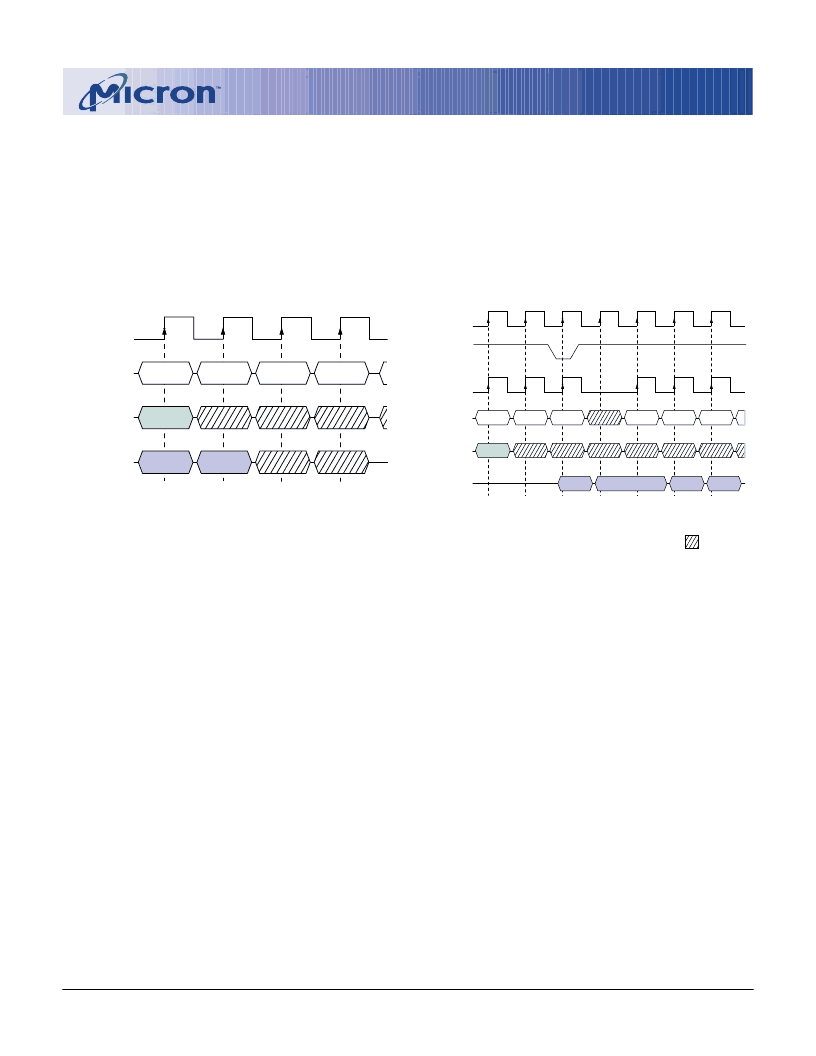
CLOCK SUSPEND
The clock suspend mode occurs when a column ac-
cess/burst is in progress and CKE is registered LOW. In
the clock suspend mode, the internal clock is deacti-
vated, “freezing” the synchronous logic.
For each positive clock edge on which CKE is
sampled LOW, the next internal positive clock edge is
suspended. Any command or data present on the in-
Figure 22
Clock Suspend During WRITE Burst
DON’T CARE
CLK
DQ
D
OUT
n
T2
T1
T4
T3
T6
T5
T0
COMMAND
ADDRESS
READ
NOP
NOP
NOP
BANK,
COL
n
NOP
D
OUT
n
+ 1
D
OUT
n
+ 2
D
OUT
n
+ 3
NOTE:
For this example, CAS latency = 2, burst length = 4 or greater, and
DQM is LOW.
CKE
INTERNAL
CLOCK
NOP
Figure 23
Clock Suspend During READ Burst
CLK
DQ
D
IN
n
T2
T1
T3
T0
COMMAND
ADDRESS
NOP
NOP
WRITE
D
IN
n
+ 1
NOP
BANK,
COL
n
NOTE:
Burst length = 2. DQM is LOW.
put pins at the time of a suspended internal clock edge
is ignored; any data present on the DQ pins remains
driven; and burst counters are not incremented, as
long as the clock is suspended. (See examples in Fig-
ures 22 and 23.)
Clock suspend mode is exited by registering CKE
HIGH; the internal clock and related operation will re-
sume on the subsequent positive clock edge.
相关PDF资料 |
PDF描述 |
|---|---|
| MT48V4M32LFFC | SYNCHRONOUS DRAM |
| MT49H16M16 | THERMISTOR PTC 100OHM 110DEG RAD |
| MT49H16M16FM | REDUCED LATENCY DRAM RLDRAM |
| MT49H8M32 | THERMISTOR PTC 100OHM 120DEG RAD |
| MT49H8M32FM | REDUCED LATENCY DRAM RLDRAM |
相关代理商/技术参数 |
参数描述 |
|---|---|
| MT48V32M16S2FG-10 | 制造商:Micron Technology Inc 功能描述:32MX16 SSDRAM PLASTIC 2BOC 2.5V - Trays |
| MT48V32M16S2FG-8 ES | 制造商:Micron Technology Inc 功能描述:DRAM CHIP MOBILE SDRAM 512MBIT 2.5V 54FBGA - Bulk |
发布紧急采购,3分钟左右您将得到回复。