- 您现在的位置:买卖IC网 > PDF目录385639 > MT48V2M32LFFC (Micron Technology, Inc.) 512K x 32 x 4 banks 2.5V SDRAM(2.5V,512K x 32 x 4组同步动态RAM) PDF资料下载
参数资料
| 型号: | MT48V2M32LFFC |
| 厂商: | Micron Technology, Inc. |
| 英文描述: | 512K x 32 x 4 banks 2.5V SDRAM(2.5V,512K x 32 x 4组同步动态RAM) |
| 中文描述: | 为512k × 32 × 4银行2.5V的内存电压(2.5V,512K采样× 32 × 4组同步动态RAM)的 |
| 文件页数: | 8/50页 |
| 文件大小: | 1058K |
| 代理商: | MT48V2M32LFFC |
第1页第2页第3页第4页第5页第6页第7页当前第8页第9页第10页第11页第12页第13页第14页第15页第16页第17页第18页第19页第20页第21页第22页第23页第24页第25页第26页第27页第28页第29页第30页第31页第32页第33页第34页第35页第36页第37页第38页第39页第40页第41页第42页第43页第44页第45页第46页第47页第48页第49页第50页
8
64Mb: x32 SDRAM, 2.5V
BatRam_25V.p65 – Rev. 0.7, Pub. 2/01
Micron Technology, Inc., reserves the right to change products or specifications without notice.
2001, Micron Technology, Inc.
64Mb: x32, 2.5V
SDRAM
PRELIMINARY
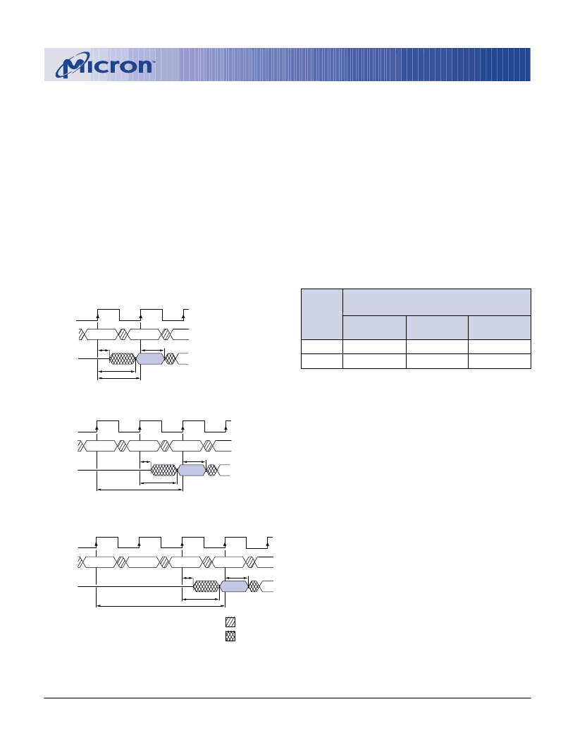
Figure 2
CAS Latency
CLK
DQ
T2
T1
T3
T0
CAS Latency = 3
LZ
t
D
OUT
tOH
COMMAND
NOP
READ
tAC
NOP
T4
NOP
DON’T CARE
UNDEFINED
CLK
DQ
T2
T1
T0
CAS Latency = 1
LZ
t
D
OUT
tOH
COMMAND
NOP
READ
tAC
CLK
DQ
T2
T1
T3
T0
CAS Latency = 2
LZ
t
D
OUT
tOH
COMMAND
NOP
READ
tAC
NOP
ALLOWABLE OPERATING
FREQUENCY (MHz)
CAS
LATENCY = 1 LATENCY = 2
£
50
£
40
CAS
CAS
SPEED
- 8
- 10
LATENCY = 3
£
125
£
100
£
100
£
76
Table 2
CAS Latency
CAS Latency
The CAS latency is the delay, in clock cycles, be-
tween the registration of a READ command and the
availability of the first piece of output data. The la-
tency can be set to one, two or three clocks.
If a READ command is registered at clock edge
n
,
and the latency is
m
clocks, the data will be available by
clock edge
n + m
. The DQs will start driving as a result of
the clock edge one cycle earlier (
n + m
- 1), and provided
that the relevant access times are met, the data will be
valid by clock edge
n + m
. For example, assuming that
the clock cycle time is such that all relevant access times
are met, if a READ command is registered at T0 and the
latency is programmed to two clocks, the DQs will start
driving after T1 and the data will be valid by T2, as
shown in Figure 2. Table 2 below indicates the operat-
ing frequencies at which each CAS latency setting can
be used.
Reserved states should not be used as unknown
operation or incompatibility with future versions may
result.
Operating Mode
The normal operating mode is selected by setting
M7 to zero; the other combinations of values for M7 are
reserved for future use and/or test modes. The pro-
grammed burst length applies to both READ and
WRITE bursts.
Test modes and reserved states should not be used
because unknown operation or incompatibility with
future versions may result.
Self Refresh Rate Select
Every cell in the DRAM requires refreshing due to
the capacitor losing its charge over time. The refresh
rate is dependent on temperature. At higher tempera-
tures the capacitors lose charge quicker, requiring the
cells to be refreshed more often. Historically, during
Self Refresh, the refresh rate is set to accomodate the
worst case, or highest temperature range expected.
Thus, during ambiant temperatures, the power con-
sumed during refresh is unnecessarily high, because
the refresh rate was set to accommodate the higher
temperatures. Setting M12 and M11, allow the DRAM
to accomodate more specific temperature regions dur-
ing SELF REFRESH. There are three temperature set-
tings, which will vary the SELF REFRESH current ac-
cording to the selected temperature. This selectable
refresh rate will save power when the DRAM is operat-
ing at normal temperatures.
相关PDF资料 |
PDF描述 |
|---|---|
| MT48V4M32LFFC | SYNCHRONOUS DRAM |
| MT49H16M16 | THERMISTOR PTC 100OHM 110DEG RAD |
| MT49H16M16FM | REDUCED LATENCY DRAM RLDRAM |
| MT49H8M32 | THERMISTOR PTC 100OHM 120DEG RAD |
| MT49H8M32FM | REDUCED LATENCY DRAM RLDRAM |
相关代理商/技术参数 |
参数描述 |
|---|---|
| MT48V32M16S2FG-10 | 制造商:Micron Technology Inc 功能描述:32MX16 SSDRAM PLASTIC 2BOC 2.5V - Trays |
| MT48V32M16S2FG-8 ES | 制造商:Micron Technology Inc 功能描述:DRAM CHIP MOBILE SDRAM 512MBIT 2.5V 54FBGA - Bulk |
发布紧急采购,3分钟左右您将得到回复。