- 您现在的位置:买卖IC网 > PDF目录299768 > PF38F40L0YUQ0 (NUMONYX) 16M X 16 FLASH 1.8V PROM, PBGA88 PDF资料下载
参数资料
| 型号: | PF38F40L0YUQ0 |
| 厂商: | NUMONYX |
| 元件分类: | PROM |
| 英文描述: | 16M X 16 FLASH 1.8V PROM, PBGA88 |
| 封装: | 8 X 11 MM, 1 MM HEIGHT, ROHS COMPLIANT, VFBGA-88 |
| 文件页数: | 41/99页 |
| 文件大小: | 1419K |
| 代理商: | PF38F40L0YUQ0 |
第1页第2页第3页第4页第5页第6页第7页第8页第9页第10页第11页第12页第13页第14页第15页第16页第17页第18页第19页第20页第21页第22页第23页第24页第25页第26页第27页第28页第29页第30页第31页第32页第33页第34页第35页第36页第37页第38页第39页第40页当前第41页第42页第43页第44页第45页第46页第47页第48页第49页第50页第51页第52页第53页第54页第55页第56页第57页第58页第59页第60页第61页第62页第63页第64页第65页第66页第67页第68页第69页第70页第71页第72页第73页第74页第75页第76页第77页第78页第79页第80页第81页第82页第83页第84页第85页第86页第87页第88页第89页第90页第91页第92页第93页第94页第95页第96页第97页第98页第99页
Intel StrataFlash Wireless Memory (L18)
Intel StrataFlash Wireless Memory (L18) with A/D-Multiplexed I/O
Datasheet
July 2006
46
Order Number: 313295-002US
10.3.1
Read Mode
The Read Mode (RM) bit selects synchronous burst-mode or asynchronous read-mode
operation for the device. When the RM bit is set, asynchronous read mode is selected
(default). When RM is cleared, synchronous burst mode is selected.
10.3.2
Latency Count
The Latency Count bits, LC[2:0], tell the device how many clock cycles must elapse
from the rising edge of ADV# or from the first valid clock edge after ADV# is asserted
before the WAIT signal indicates valid data is present on the device data signals
AD[15:0]. The input clock frequency determines this value. Figure 16 shows the data
output latency from ADV#-asserted for different settings of LC[2:0]. The Latency Count
does not affect when data becomes available on the data signals. Valid data is driven
onto the data bus, with respect to a valid clock edge, as soon as possible after the
asynchronous access time is satisfied (or another word after it is sensed). In this way,
the data “flows-through” on the first access, with respect to an active clock edge. The
data continues to be available on the data bus until the latency period is over. The flow-
through behavior only applies to the first access of any bus cycle. All subsequent data
is driven on valid clock edges following the first access latency period.
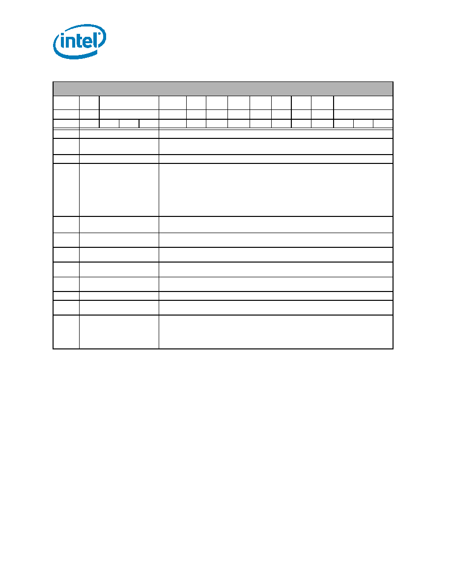
Table 15. Read Configuration Register Description
Read Configuration Register (RCR)
Read
Mode
RES
Latency Count
WAIT
Polarity
Data
Hold
WAIT
Delay
Burst
Seq
CLK
Edge
RES
Burst
Wrap
Burst Length
RM
R
LC[2:0]
WP
DH
WD
BS
CE
R
BW
BL[2:0]
15
14
13
12
11
10
9
8
7
6
5
4
3
2
1
0
Bit
Name
Description
15
Read Mode (RM)
0 = Synchronous burst-mode read
1 = Asynchronous read (default)
14
Reserved (R)
Reserved bits should be cleared (0)
13:11
Latency Count (LC[2:0])
010 =Code 2
011 =Code 3
100 =Code 4
101 =Code 5
110 =Code 6
111 =Code 7(default)
(Other bit settings are reserved)
10
Wait Polarity (WP)
0 =WAIT signal is active low
1 =WAIT signal is active high (default)
9
Data Hold (DH)
0 =Data held for a 1-clock data cycle
1 =Data held for a 2-clock data cycle (default)
8
Wait Delay (WD)
0 =WAIT de-asserted with valid data
1 =WAIT de-asserted one data cycle before valid data (default)
7
Burst Sequence (BS)
0 =Reserved
1 =Linear (default)
6
Clock Edge (CE)
0 = Falling edge
1 = Rising edge (default)
5:4
Reserved (R)
Reserved bits should be cleared (0)
3Burst Wrap (BW)
0 =Wrap; Burst accesses wrap within burst length set by BL[2:0]
1 =No Wrap; Burst accesses do not wrap within burst length (default)
2:0
Burst Length (BL[2:0])
001 =4-word burst
010 =8-word burst
011 =16-word burst
111 =Continuous-word burst (default)
(Other bit settings are reserved)
相关PDF资料 |
PDF描述 |
|---|---|
| PF50WIW2K-3.5VF-W6 | SINGLE COLOR LED, INCAND WHITE |
| PD50WO3K-28V-T | SINGLE COLOR LED, SUPER ORANGE |
| PD50WR3K-24V-W6 | SINGLE COLOR LED, ULTRA RED |
| PF50WAG6K-240VAC-W6 | SINGLE COLOR LED, AQUA GREEN |
| PF50WW1K-12V-W6 | SINGLE COLOR LED, COOL WHITE |
相关代理商/技术参数 |
参数描述 |
|---|---|
| PF38F4470LLYBBEA | 制造商:Micron Technology Inc 功能描述:256LCR/256LCR/256SD SCSP 1.8 X16D LF - Trays |
| PF38F5050M0Y0CFA | 制造商:Micron Technology Inc 功能描述:512BA/64PS SCSP 1.8 LF MICRON - Trays |
| PF38F5050M0Y0CFB | 制造商:Micron Technology Inc 功能描述:512BA/64PS SCSP 1.8 LF MICRON - Tape and Reel |
| PF38F5050M0Y0CGA | 制造商:Micron Technology Inc 功能描述:512BA/64PS SCSP 1.8 LF MICRON - Trays |
| PF38F5060M0Y0BEA | 功能描述:IC FLASH 512MBIT 133MHZ 105SCSP RoHS:是 类别:集成电路 (IC) >> 存储器 系列:- 标准包装:3,000 系列:- 格式 - 存储器:EEPROMs - 串行 存储器类型:EEPROM 存储容量:32K (4K x 8) 速度:100kHz,400kHz 接口:I²C,2 线串口 电源电压:2.5 V ~ 5.5 V 工作温度:-40°C ~ 125°C 封装/外壳:8-SOIC(0.154",3.90mm 宽) 供应商设备封装:8-SOIC 包装:带卷 (TR) 其它名称:CAV24C32WE-GT3OSTR |
发布紧急采购,3分钟左右您将得到回复。