- 您现在的位置:买卖IC网 > PDF目录225025 > RC28F160C3BD70 (INTEL CORP) 1M X 16 FLASH 3V PROM, 70 ns, PBGA64 PDF资料下载
参数资料
| 型号: | RC28F160C3BD70 |
| 厂商: | INTEL CORP |
| 元件分类: | PROM |
| 英文描述: | 1M X 16 FLASH 3V PROM, 70 ns, PBGA64 |
| 封装: | BGA-64 |
| 文件页数: | 33/72页 |
| 文件大小: | 1083K |
| 代理商: | RC28F160C3BD70 |
第1页第2页第3页第4页第5页第6页第7页第8页第9页第10页第11页第12页第13页第14页第15页第16页第17页第18页第19页第20页第21页第22页第23页第24页第25页第26页第27页第28页第29页第30页第31页第32页当前第33页第34页第35页第36页第37页第38页第39页第40页第41页第42页第43页第44页第45页第46页第47页第48页第49页第50页第51页第52页第53页第54页第55页第56页第57页第58页第59页第60页第61页第62页第63页第64页第65页第66页第67页第68页第69页第70页第71页第72页
Intel Advanced+ Boot Block Flash Memory (C3)
Datasheet
Intel Advanced+ Boot Block Flash Memory (C3)
May 2005
Order Number: 290645, Revision: 023
39
9.0
Device Operations
The Intel Advanced+ Boot Block Flash Memory (C3) device uses a CUI and automated
algorithms to simplify Program and Erase operations. The CUI allows for 100% CMOS-level
control inputs and fixed power supplies during erasure and programming.
The internal WSM completely automates Program and Erase operations while the CUI signals the
start of an operation and the Status Register reports device status. The CUI handles the WE#
interface to the data and address latches as well as system status requests during WSM operation.
9.1
Bus Operations
The Intel Advanced+ Boot Block Flash Memory (C3) device performs read, program, and erase
operations in-system through the local CPU or microcontroller. Four control pins (CE#, OE#,
WE#, and RP#) manage the data flow in and out of the flash device. Table 20 on page 39
summarizes these bus operations.
9.1.1
Read
When performing a read cycle, CE# and OE# must be asserted; WE# and RP# must be deasserted.
CE# is the device selection control; when active low, it enables the flash memory device. OE# is
the data output control; when low, data is output on DQ[15:0]. See Figure 9, “Read Operation
9.1.2
Write
A write cycle occurs when both CE# and WE# are low; RP# and OE# are high. Commands are
issued to the Command User Interface (CUI). The CUI does not occupy an addressable memory
location. Address and data are latched on the rising edge of the WE# or CE# pulse, whichever
occurs first. See Figure 10, “Write Operations Waveform” on page 32.
9.1.3
Output Disable
With OE# at a logic-high level (VIH), the device outputs are disabled. DQ[15:0] are placed in a
high-impedance state.
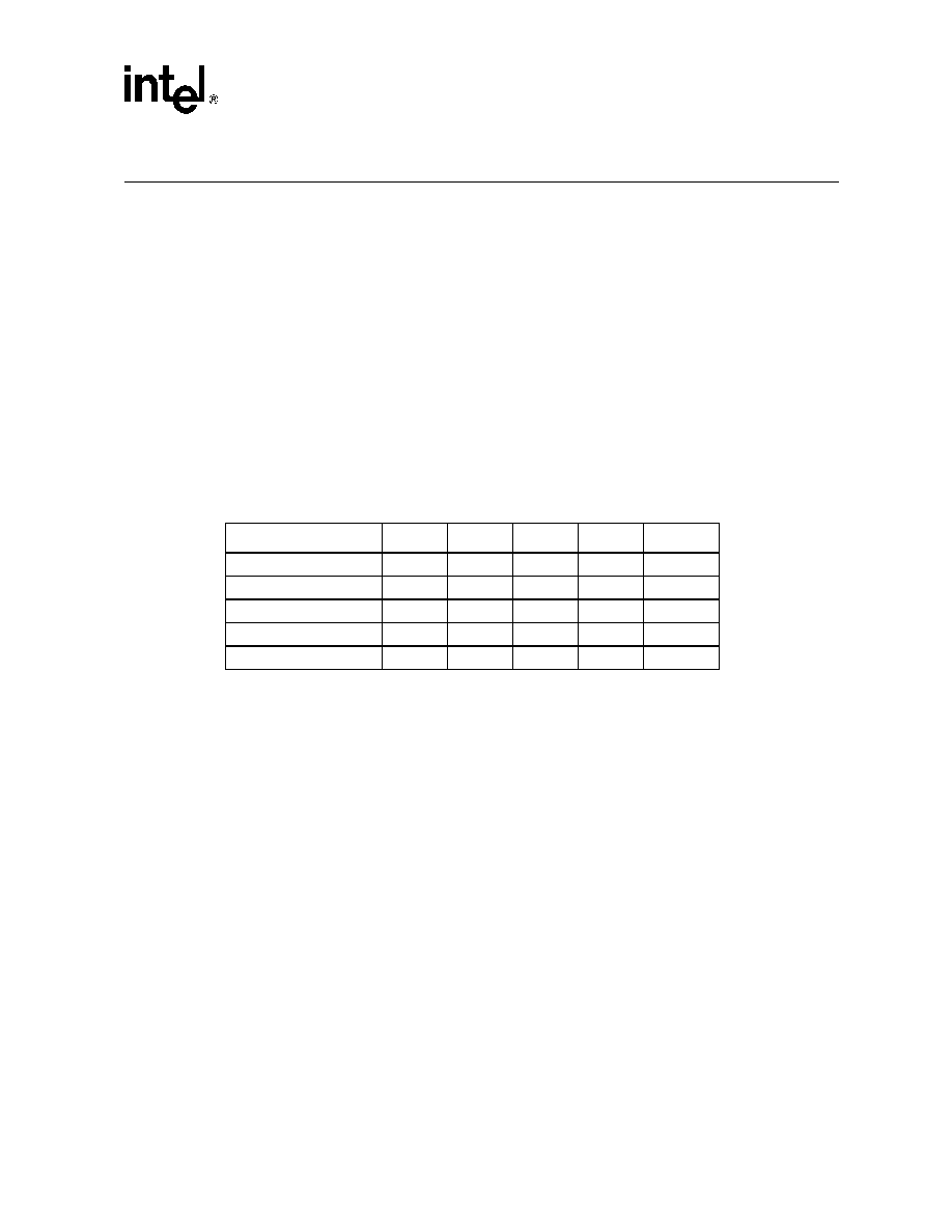
Table 20.
Bus Operations
Mode
RP#
CE#
OE#
WE#
DQ[15:0]
Read
VIH
VIL
VIH
DOUT
Write
VIH
VIL
VIH
VIL
DIN
Output Disable
VIH
VIL
VIH
High-Z
Standby
VIH
XX
High-Z
Reset
VIL
XX
X
High-Z
Note:
X = Don’t Care (VIL or VIH)
相关PDF资料 |
PDF描述 |
|---|---|
| RC4194K | DUAL OUTPUT, ADJUSTABLE MIXED REGULATOR, MBFM9 |
| RM4194K | DUAL OUTPUT, ADJUSTABLE MIXED REGULATOR, MBFM9 |
| RC4194D | DUAL OUTPUT, ADJUSTABLE MIXED REGULATOR, CDIP14 |
| RM4194D/883B | DUAL OUTPUT, ADJUSTABLE MIXED REGULATOR, CDIP14 |
| RM4194D | DUAL OUTPUT, ADJUSTABLE MIXED REGULATOR, CDIP14 |
相关代理商/技术参数 |
参数描述 |
|---|---|
| RC28F160C3BD70A | 功能描述:IC FLASH 16MBIT 70NS 64BGA RoHS:否 类别:集成电路 (IC) >> 存储器 系列:- 标准包装:96 系列:- 格式 - 存储器:闪存 存储器类型:FLASH 存储容量:16M(2M x 8,1M x 16) 速度:70ns 接口:并联 电源电压:2.65 V ~ 3.6 V 工作温度:-40°C ~ 85°C 封装/外壳:48-TFSOP(0.724",18.40mm 宽) 供应商设备封装:48-TSOP 包装:托盘 |
| RC28F160C3TA110 | 制造商:INTEL 制造商全称:Intel Corporation 功能描述:Advanced+ Boot Block Flash Memory (C3) |
| RC28F160C3TA70 | 制造商:INTEL 制造商全称:Intel Corporation 功能描述:Advanced+ Boot Block Flash Memory (C3) |
| RC28F160C3TA90 | 制造商:INTEL 制造商全称:Intel Corporation 功能描述:Advanced+ Boot Block Flash Memory (C3) |
| RC28F160C3TA90SB93 | 功能描述:IC FLASH 16MBIT 90NS 64BGA RoHS:否 类别:集成电路 (IC) >> 存储器 系列:- 标准包装:150 系列:- 格式 - 存储器:EEPROMs - 串行 存储器类型:EEPROM 存储容量:4K (2 x 256 x 8) 速度:400kHz 接口:I²C,2 线串口 电源电压:2.5 V ~ 5.5 V 工作温度:-40°C ~ 85°C 封装/外壳:8-VFDFN 裸露焊盘 供应商设备封装:8-DFN(2x3) 包装:管件 产品目录页面:1445 (CN2011-ZH PDF) |
发布紧急采购,3分钟左右您将得到回复。