- 您现在的位置:买卖IC网 > PDF目录225025 > RC28F160C3BD70 (INTEL CORP) 1M X 16 FLASH 3V PROM, 70 ns, PBGA64 PDF资料下载
参数资料
| 型号: | RC28F160C3BD70 |
| 厂商: | INTEL CORP |
| 元件分类: | PROM |
| 英文描述: | 1M X 16 FLASH 3V PROM, 70 ns, PBGA64 |
| 封装: | BGA-64 |
| 文件页数: | 63/72页 |
| 文件大小: | 1083K |
| 代理商: | RC28F160C3BD70 |
第1页第2页第3页第4页第5页第6页第7页第8页第9页第10页第11页第12页第13页第14页第15页第16页第17页第18页第19页第20页第21页第22页第23页第24页第25页第26页第27页第28页第29页第30页第31页第32页第33页第34页第35页第36页第37页第38页第39页第40页第41页第42页第43页第44页第45页第46页第47页第48页第49页第50页第51页第52页第53页第54页第55页第56页第57页第58页第59页第60页第61页第62页当前第63页第64页第65页第66页第67页第68页第69页第70页第71页第72页
Intel Advanced+ Boot Block Flash Memory (C3)
May 2005
Intel Advanced+ Boot Block Flash Memory (C3)
Datasheet
66
Order Number: 290645, Revision: 023
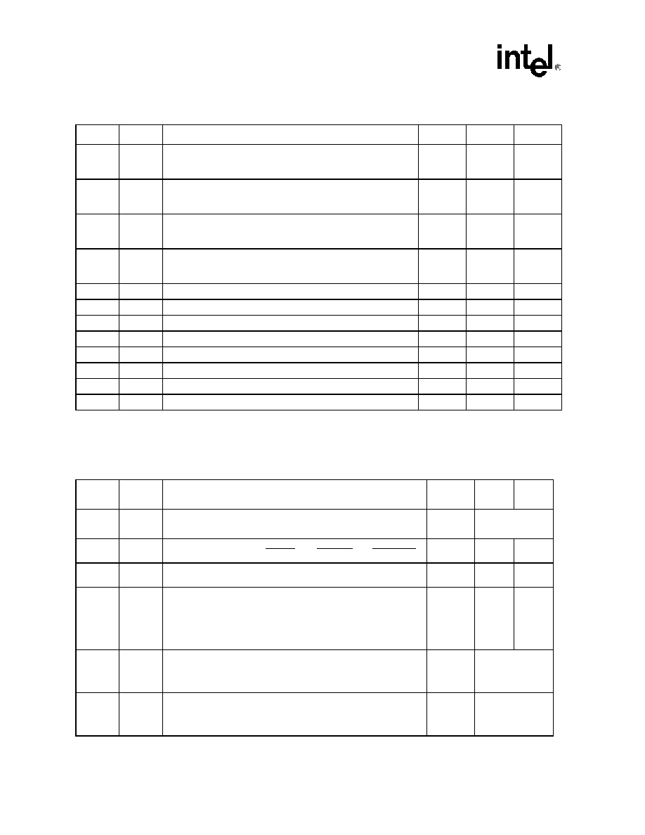
Table 32.
System Interface Information
C.5
Device Geometry Definition
Table 33.
Device Geometry Definition
Offset
Length
Description
Add.
Hex Code
Value
0x1B
1
VCC logic supply minimum program/erase voltage
bits 0–3 BCD 100 mV
bits 4–7 BCD volts
1B:
--27
2.7 V
0x1C
1
VCC logic supply maximum program/erase voltage
bits 0–3 BCD 100 mV
bits 4–7 BCD volts
1C:
--36
3.6 V
0x1D
1
VPP [programming] supply minimum program/erase voltage
bits 0–3 BCD 100 mV
bits 4–7 HEX volts
1D:
--B4
11.4 V
0x1E
1
VPP [programming] supply maximum program/erase voltage
bits 0–3 BCD 100 mV
bits 4–7 HEX volts
1E:
--C6
12.6 V
0x1F
1
“n” such that typical single word program time-out =2
n s
1F:
--05
32 s
0x20
1
“n” such that typical max. buffer write time-out = 2n s
20:
--00
NA
0x21
1
“n” such that typical block erase time-out = 2
n ms
21:
--0A
1 s
0x22
1
“n” such that typical full chip erase time-out = 2n ms
22:
--00
NA
0x23
1
“n” such that maximum word program time-out = 2
n times typical
23:
--04
512s
0x24
1
“n” such that maximum buffer write time-out = 2n times typical
24:
--00
NA
0x25
1
“n” such that maximum block erase time-out = 2
n times typical
25:
--03
8s
0x26
1
“n” such that maximum chip erase time-out = 2n times typical
26:
--00
NA
Offset
Length
Description
Add.
Hex
Code
Value
0x27
1
“n” such that device size = 2
n in number of bytes
27
0x28
2
Flash device interface:
x8 async
28:00,29:00
x16 async
28:01,29:00
x8/x16 async
28:02,29:00
28:
29:
--01
--00
x16
0x2A
2
“n” such that maximum number of bytes in write buffer = 2
n
2A:
2B:
--00
0
0x2C
1
Number of erase block regions within device:
1. x = 0 means no erase blocking; the device erases in “bulk”
2. x specifies the number of device or partition regions
with one or more contiguous same-size erase blocks.
3. Symmetrically blocked partitions have one blocking region
4. Partition size = (total blocks) x (individual block size)
2C:
--02
2
0x2D
4
Erase Block Region 1 Information
bits 0–15 = y, y+1 = number of identical-size erase blocks
bits 16–31 = z, region erase block(s) size are z x 256 bytes
2D:
2E:
2F:
30:
0x2D
14
Erase Block Region 2 Information
bits 0–15 = y, y+1 = number of identical-size erase blocks
bits 16–31 = z, region erase block(s) size are z x 256 bytes
31:
32:
33:
34:
相关PDF资料 |
PDF描述 |
|---|---|
| RC4194K | DUAL OUTPUT, ADJUSTABLE MIXED REGULATOR, MBFM9 |
| RM4194K | DUAL OUTPUT, ADJUSTABLE MIXED REGULATOR, MBFM9 |
| RC4194D | DUAL OUTPUT, ADJUSTABLE MIXED REGULATOR, CDIP14 |
| RM4194D/883B | DUAL OUTPUT, ADJUSTABLE MIXED REGULATOR, CDIP14 |
| RM4194D | DUAL OUTPUT, ADJUSTABLE MIXED REGULATOR, CDIP14 |
相关代理商/技术参数 |
参数描述 |
|---|---|
| RC28F160C3BD70A | 功能描述:IC FLASH 16MBIT 70NS 64BGA RoHS:否 类别:集成电路 (IC) >> 存储器 系列:- 标准包装:96 系列:- 格式 - 存储器:闪存 存储器类型:FLASH 存储容量:16M(2M x 8,1M x 16) 速度:70ns 接口:并联 电源电压:2.65 V ~ 3.6 V 工作温度:-40°C ~ 85°C 封装/外壳:48-TFSOP(0.724",18.40mm 宽) 供应商设备封装:48-TSOP 包装:托盘 |
| RC28F160C3TA110 | 制造商:INTEL 制造商全称:Intel Corporation 功能描述:Advanced+ Boot Block Flash Memory (C3) |
| RC28F160C3TA70 | 制造商:INTEL 制造商全称:Intel Corporation 功能描述:Advanced+ Boot Block Flash Memory (C3) |
| RC28F160C3TA90 | 制造商:INTEL 制造商全称:Intel Corporation 功能描述:Advanced+ Boot Block Flash Memory (C3) |
| RC28F160C3TA90SB93 | 功能描述:IC FLASH 16MBIT 90NS 64BGA RoHS:否 类别:集成电路 (IC) >> 存储器 系列:- 标准包装:150 系列:- 格式 - 存储器:EEPROMs - 串行 存储器类型:EEPROM 存储容量:4K (2 x 256 x 8) 速度:400kHz 接口:I²C,2 线串口 电源电压:2.5 V ~ 5.5 V 工作温度:-40°C ~ 85°C 封装/外壳:8-VFDFN 裸露焊盘 供应商设备封装:8-DFN(2x3) 包装:管件 产品目录页面:1445 (CN2011-ZH PDF) |
发布紧急采购,3分钟左右您将得到回复。