- 您现在的位置:买卖IC网 > PDF目录225025 > RC28F160C3BD70 (INTEL CORP) 1M X 16 FLASH 3V PROM, 70 ns, PBGA64 PDF资料下载
参数资料
| 型号: | RC28F160C3BD70 |
| 厂商: | INTEL CORP |
| 元件分类: | PROM |
| 英文描述: | 1M X 16 FLASH 3V PROM, 70 ns, PBGA64 |
| 封装: | BGA-64 |
| 文件页数: | 48/72页 |
| 文件大小: | 1083K |
| 代理商: | RC28F160C3BD70 |
第1页第2页第3页第4页第5页第6页第7页第8页第9页第10页第11页第12页第13页第14页第15页第16页第17页第18页第19页第20页第21页第22页第23页第24页第25页第26页第27页第28页第29页第30页第31页第32页第33页第34页第35页第36页第37页第38页第39页第40页第41页第42页第43页第44页第45页第46页第47页当前第48页第49页第50页第51页第52页第53页第54页第55页第56页第57页第58页第59页第60页第61页第62页第63页第64页第65页第66页第67页第68页第69页第70页第71页第72页
Intel Advanced+ Boot Block Flash Memory (C3)
May 2005
Intel Advanced+ Boot Block Flash Memory (C3)
Datasheet
52
Order Number: 290645, Revision: 023
11.5.1
Reading the Protection Register
The protection register is read in the Read-Identifier mode. The device is switched to this mode by
issuing the Read Identifier command (0x90). Once in this mode, read cycles from addresses shown
in Figure 15, “Protection Register Mapping” retrieve the specified information. To return to Read-
Array mode, issue the Read Array command (0xFF).
11.5.2
Programming the Protection Register
The protection register bits are programmed using the two-cycle Protection Program command.
The 64-bit number is programmed 16 bits at a time. First, issue the Protection Program Setup
command, 0xC0. The next write to the device will latch in address and data and program the
specified location. The allowable addresses are listed in Table 21, “Device Identification Codes”
to program to a previously locked protection register segment will result in a Status Register error
(Program Error bit SR[4] and Lock Error bit SR[1] will be set to 1).
Note:
Do not attempt to address Protection Program commands outside the defined protection register
address space; status register can be indeterminate.
11.5.3
Locking the Protection Register
The user-programmable segment of the protection register is lockable by programming bit 1 of the
PR-LOCK location to 0. See Figure 15, “Protection Register Mapping” on page 52. Bit 0 of this
location is programmed to 0 at the Intel factory to protect the unique device number. This bit is set
using the Protection Program command to program 0xFFFD to the PR-LOCK location. After these
bits have been programmed, no further changes can be made to the values stored in the protection
register. Protection Program commands to a locked section will result in a Status Register error
(Program Error bit SR[4] and Lock Error bit SR[1] will be set to 1). Protection register lockout
state is not reversible.
11.6
VPP Program and Erase Voltages
The C3 device provides in-system programming and erase in the 1.65 V–3.6 V range. For fast
production programming, 12 V programming can be used. See Figure 16, “Example Power Supply
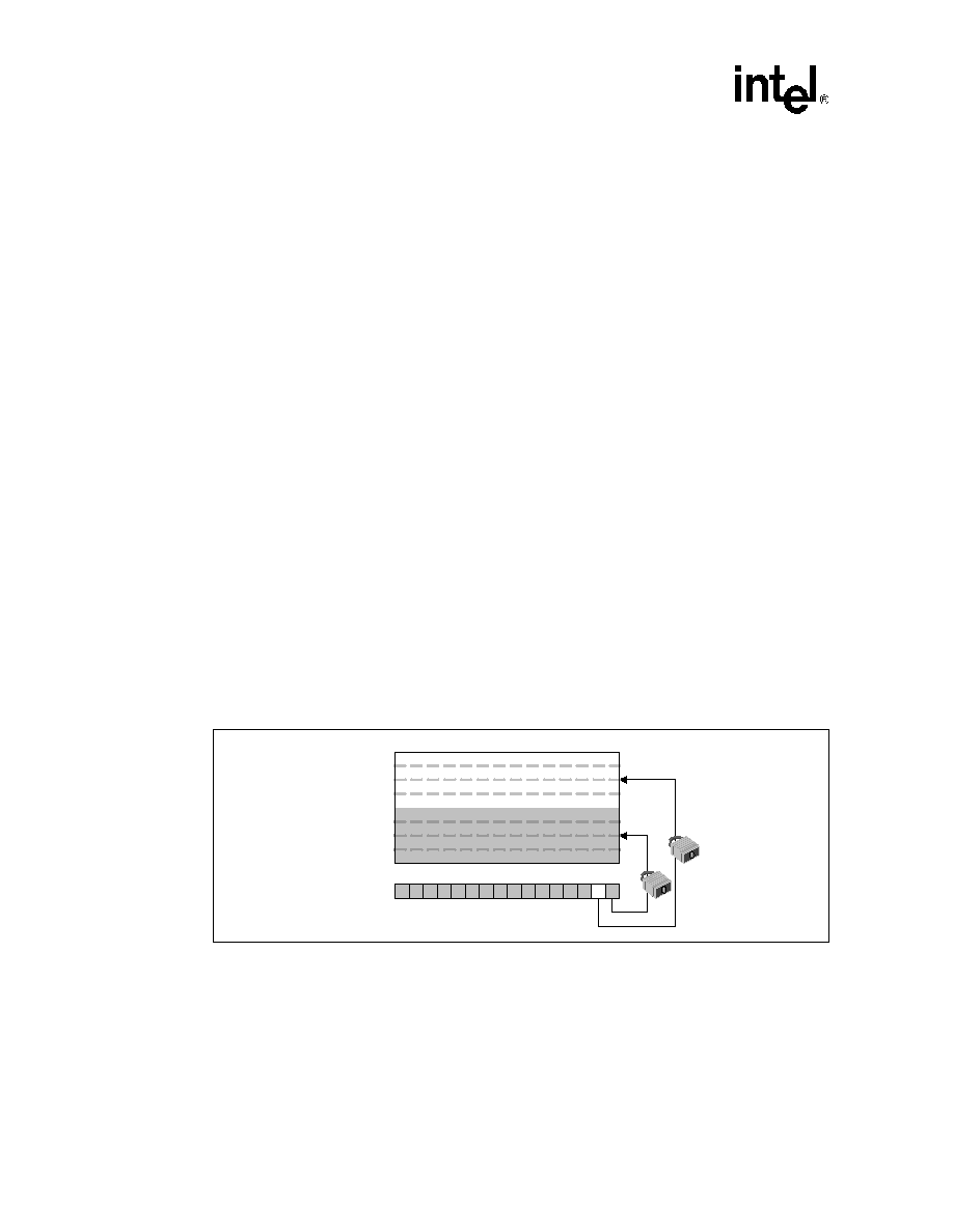
Figure 15.
Protection Register Mapping
0x88
0x85
64-bit Segment
(User-Programmable)
0x84
0x81
0x80
PR Lock Register 0
64-bit Segment
(Intel Factory-Programmed)
15 14 13 12 11 10 9
8
7
6
5
4
3
2
1
0
128-Bit Protection Register 0
相关PDF资料 |
PDF描述 |
|---|---|
| RC4194K | DUAL OUTPUT, ADJUSTABLE MIXED REGULATOR, MBFM9 |
| RM4194K | DUAL OUTPUT, ADJUSTABLE MIXED REGULATOR, MBFM9 |
| RC4194D | DUAL OUTPUT, ADJUSTABLE MIXED REGULATOR, CDIP14 |
| RM4194D/883B | DUAL OUTPUT, ADJUSTABLE MIXED REGULATOR, CDIP14 |
| RM4194D | DUAL OUTPUT, ADJUSTABLE MIXED REGULATOR, CDIP14 |
相关代理商/技术参数 |
参数描述 |
|---|---|
| RC28F160C3BD70A | 功能描述:IC FLASH 16MBIT 70NS 64BGA RoHS:否 类别:集成电路 (IC) >> 存储器 系列:- 标准包装:96 系列:- 格式 - 存储器:闪存 存储器类型:FLASH 存储容量:16M(2M x 8,1M x 16) 速度:70ns 接口:并联 电源电压:2.65 V ~ 3.6 V 工作温度:-40°C ~ 85°C 封装/外壳:48-TFSOP(0.724",18.40mm 宽) 供应商设备封装:48-TSOP 包装:托盘 |
| RC28F160C3TA110 | 制造商:INTEL 制造商全称:Intel Corporation 功能描述:Advanced+ Boot Block Flash Memory (C3) |
| RC28F160C3TA70 | 制造商:INTEL 制造商全称:Intel Corporation 功能描述:Advanced+ Boot Block Flash Memory (C3) |
| RC28F160C3TA90 | 制造商:INTEL 制造商全称:Intel Corporation 功能描述:Advanced+ Boot Block Flash Memory (C3) |
| RC28F160C3TA90SB93 | 功能描述:IC FLASH 16MBIT 90NS 64BGA RoHS:否 类别:集成电路 (IC) >> 存储器 系列:- 标准包装:150 系列:- 格式 - 存储器:EEPROMs - 串行 存储器类型:EEPROM 存储容量:4K (2 x 256 x 8) 速度:400kHz 接口:I²C,2 线串口 电源电压:2.5 V ~ 5.5 V 工作温度:-40°C ~ 85°C 封装/外壳:8-VFDFN 裸露焊盘 供应商设备封装:8-DFN(2x3) 包装:管件 产品目录页面:1445 (CN2011-ZH PDF) |
发布紧急采购,3分钟左右您将得到回复。