- 您现在的位置:买卖IC网 > PDF目录192292 > S19237PB13 (APPLIEDMICRO INC) TRANSCEIVER, PBGA255 PDF资料下载
参数资料
| 型号: | S19237PB13 |
| 厂商: | APPLIEDMICRO INC |
| 元件分类: | 数字传输电路 |
| 英文描述: | TRANSCEIVER, PBGA255 |
| 封装: | PLASTIC, BGA-255 |
| 文件页数: | 22/60页 |
| 文件大小: | 1418K |
| 代理商: | S19237PB13 |
第1页第2页第3页第4页第5页第6页第7页第8页第9页第10页第11页第12页第13页第14页第15页第16页第17页第18页第19页第20页第21页当前第22页第23页第24页第25页第26页第27页第28页第29页第30页第31页第32页第33页第34页第35页第36页第37页第38页第39页第40页第41页第42页第43页第44页第45页第46页第47页第48页第49页第50页第51页第52页第53页第54页第55页第56页第57页第58页第59页第60页
S19237 – SONET STS-192/10GbE CMOS Transceiver
with ISI Compensation
AMCC Confidential and Proprietary
DS1454
29
Data Sheet
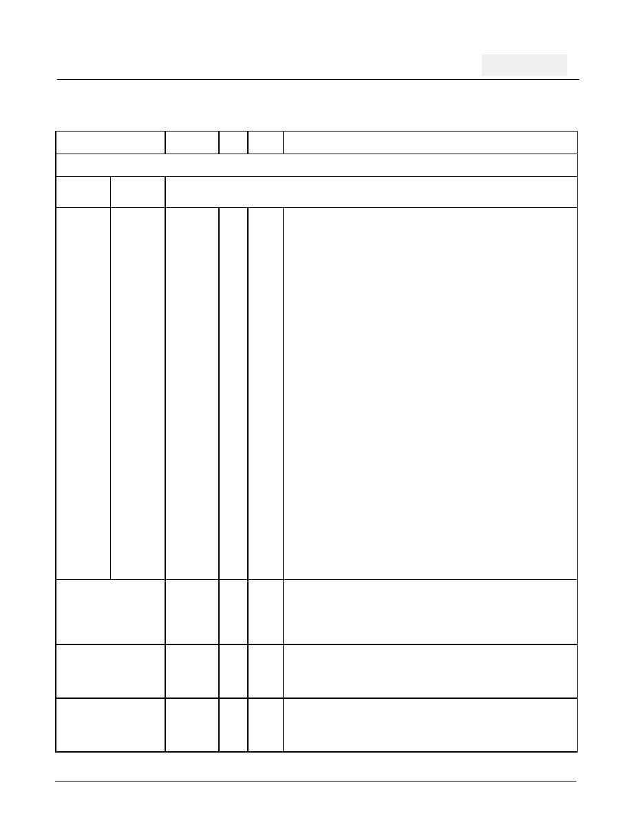
PIN ASSIGNMENTS AND DESCRIPTIONS
Table 17. Input Pin Assignments and Descriptions
Pin Name
Level
I/O
Pin#
Description
TRANSMITTER INPUTS
DATA_
SWAP = 0
DATA_
SWAP = 1
PINP0
PINN0
PINP1
PINN1
PINP2
PINN2
PINP3
PINN3
PINP4
PINN4
PINP5
PINN5
PINP6
PINN6
PINP7
PINN7
PINP8
PINN8
PINP9
PINN9
PINP10
PINN10
PINP11
PINN11
PINP12
PINN12
PINP13
PINN13
PINP14
PINN14
PINP15
PINN15
PINP15
PINN15
PINP14
PINN14
PINP13
PINN13
PINP12
PINN12
PINP11
PINN11
PINP10
PINN10
PINP9
PINN9
PINP8
PINN8
PINP7
PINN7
PINP6
PINN6
PINP5
PINN5
PINP4
PINN4
PINP3
PINN3
PINP2
PINN2
PINP1
PINN1
PINP0
PINN0
LVDS
I
D11
D12
C12
C11
B12
B11
A12
A11
H14
G14
F14
E14
D14
C14
B14
A14
H15
G15
E15
F15
D15
C15
B15
A15
H16
G16
F16
E16
D16
C16
B16
A16
Parallel Data Input. A 16-bit parallel 622.08 Mbps. (or equivalent
FEC/10 Gigabit Ethernet rate) word, aligned to the Parallel Input
Clock (PICLK). PINP/N[15] is the most significant bit (corresponding
to bit 1 of each word, the first bit transmitted). PINP/N[0] is the least
significant bit (corresponding to bit 16 of each word, the last bit trans-
mitted). PINP/N[15:0] is sampled on the rising edge of PICLK. Inter-
nally terminated 100
line-to-line. This input is not internally biased.
PICLKP
PICLKN
LVDS
I
B13
A13
Parallel Input Clock. A 622.08 MHz nominally 50% duty cycle input
clock, to which PINP/N[15:0] is aligned. PICLK is used to transfer the
data on the PIN inputs into a FIFO and holding register in the paral-
lel-to-serial converter. Internally terminated 100
line to line. This
input is not internally biased.
TSDAMPADJ
MDIO
I
Transmit Serial Data Output Amplitude Adjust. Used to program
the serial data output differential voltage swing levels. See Table 3,
TSD Output Swing Select, for voltage levels. This signal can be
accessed through the MDIO bus register (Default = 1).
CSU_REFCLKP
CSU_REFCLKN
REFCLK
Diff CML
I
A3
A2
Transmit Reference Clock. Input used as the reference for the
internal bit clock frequency synthesizer. This input is internally biased
and terminated. This input must be AC coupled. See Table 1 for dif-
ferent CSU_REFCLK rates.
相关PDF资料 |
PDF描述 |
|---|---|
| S1950E-FREQ-OUT25 | CRYSTAL OSCILLATOR, CLOCK, 80 MHz - 125 MHz, ACMOS OUTPUT |
| S1F78100Y2A0 | 6 V FIXED POSITIVE REGULATOR, PSSO3 |
| S1F78100Y2B0 | 5 V FIXED POSITIVE REGULATOR, PSSO3 |
| S1F78100Y2C0 | 3.2 V FIXED POSITIVE REGULATOR, PSSO3 |
| S1F78100Y2F0 | 2.2 V FIXED POSITIVE REGULATOR, PSSO3 |
相关代理商/技术参数 |
参数描述 |
|---|---|
| S19237PB13-2 | 制造商:AppliedMicro 功能描述: |
| S19237PBICC | 制造商:AppliedMicro 功能描述:IC INTERFACE TRANSCEIVER LOW POWER CMOS 255 BGA 制造商:AMCC 功能描述: |
| S19238CBI | 制造商:AppliedMicro 功能描述: |
| S19250 | 制造商:AMCC 制造商全称:Applied Micro Circuits Corporation 功能描述:STS-192 SONET/SDH/FEC/GbE/FC 16-bit Transceiver with EDC |
| S19250PBIC | 制造商:AppliedMicro 功能描述:10G SERDES EDC/SFI-4 |
发布紧急采购,3分钟左右您将得到回复。