- 您现在的位置:买卖IC网 > PDF目录192292 > S19237PB13 (APPLIEDMICRO INC) TRANSCEIVER, PBGA255 PDF资料下载
参数资料
| 型号: | S19237PB13 |
| 厂商: | APPLIEDMICRO INC |
| 元件分类: | 数字传输电路 |
| 英文描述: | TRANSCEIVER, PBGA255 |
| 封装: | PLASTIC, BGA-255 |
| 文件页数: | 5/60页 |
| 文件大小: | 1418K |
| 代理商: | S19237PB13 |
第1页第2页第3页第4页当前第5页第6页第7页第8页第9页第10页第11页第12页第13页第14页第15页第16页第17页第18页第19页第20页第21页第22页第23页第24页第25页第26页第27页第28页第29页第30页第31页第32页第33页第34页第35页第36页第37页第38页第39页第40页第41页第42页第43页第44页第45页第46页第47页第48页第49页第50页第51页第52页第53页第54页第55页第56页第57页第58页第59页第60页
S19237 – SONET STS-192/10GbE CMOS Transceiver
with ISI Compensation
AMCC Confidential and Proprietary
DS1454
13
Data Sheet
Signal Detect (SDLVCMOS) – External Pin
The signal detect is an active high or active low LVC-
MOS single-ended input to be driven by the external
optical receiver module to indicate the presence of
received optical power. When a loss-of-light condition
occurs, a de-asserted SDLVCMOS will cause the
internal PLL to be locked to the CRU_REFCLK input
signal. The SERDATIP/N (and POUT[15:0]) will be
forced to a Logic ‘0’ state when SDLVCMOS is inac-
tive. Active level (high or low) is programmed by the
SD_POL.
Signal Detect Polarity (SD_POL) – MDIO Register
The signal detect polarity is an input signal that will set
the SDLVCMOS input as either active high or active
low. Setting this pin low will set the SDLVCMOS input
as active low. Setting this pin high will set the SDLVC-
MOS input as active high. This input is only accessible
through the MDIO bus register.
Receive Reference Clock (CRU_REFCLKP/N) –
External Pin
The differential REFCLK CML 155.52 MHz (or equiva-
lent FEC/10 Gigabit Ethernet Rate) reference clock
(CRU_REFCLKP/N) input is used to establish the ini-
tial operating frequency of the Phase Lock Loop (PLL).
This input can also be driven by the 155MCKP/N out-
put from the transmit section of S19237. See Table 4,
Table 4 summarizes the increased CRU_REFCLK
rates required for the FEC operation. The S19237
incorporates the bandwidth expansion requirements
needed for FEC/10 GB Ethernet applications that pro-
vide up to eight bytes of correction per 255 byte block.
Increased CRU_REFCLK frequency is required for
bandwidth expansion due to code words and Frame
Synchronization Byte (FSB). This input is internally
biased and terminated 100 line-to-line and must be
AC coupled.
Kill Parallel Output Clock (KILLPOCLKB) –
MDIO Register
The active low Kill Parallel Output Clock (KILLPO-
CLKB) signal, when asserted low, will force the
POCLK output to a logic ‘0’ state. This input may be
programmed to logic ‘1’ for normal operation. This
input is only accessible through the MDIO bus register.
Kill Parallel Output Data (KILLPOUTB) –
MDIO Register
The active low Kill Parallel Output Data (KILLPOUTB)
signal, when asserted low, will force the POUT[15:0]
output to a logic ‘0’ state. This input may be pro-
grammed to logic ‘1’ for normal operation. This input is
only accessible through the MDIO bus register.
Kill Parallel Output MCK Clock (KILLMCKCLKB) –
MDIO Register
The active low Kill Parallel Output 622MCK Clock
(KILLMCKCLKB) signal, when asserted low, will force
the 622MCK output to a logic ‘0’ state. This input may
be programmed to logic ‘1’ for normal operation. This
input is only accessible through the MDIO bus register.
Receive Built-In Self Test Enable (RX_BIST_EN) –
MDIO Register
This active high input enables the receive built-in self
test mode. For normal system operation,
RX_BIST_EN should be programmed to logic ‘0’. The
S19237 goes in the BIST mode when RX_BIST_EN is
programmed to logic high. Once the RX_BIST_EN is
programmed to logic high, the PRBS generator will
start sending the PRBS/user defined pattern (see
Table 11 for details) through the parallel outputs, and
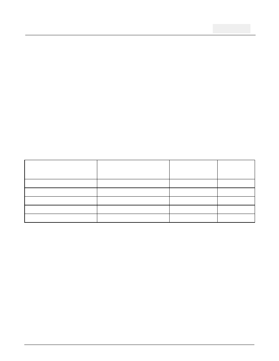
Table 4. Reference Frequency for the Clock Recovery Unit
Error Correcting Capability
Percentage Bandwidth Expansion
Due to Code Words and Frame
Synchronization Byte (FSB)
Increased Receive
Data Input (SERDATI)
Frequency
Required
(CRU_REFCLK)
Frequency
STS-192, 0 bytes
0% increase
9.953 Gbps
155.52 MHz
STS-192, Reed Soloman - 255/238
7.14% increase
10.664 Gbps
166.63 MHz
STS-192, Reed Soloman - 255/237
7.59% increase
10.709 Gbps
167.33 MHz
10 Gigabit Ethernet
0% increase
10.000 Gbps
156.25 MHz
10 Gigabit Ethernet 64/66B Encoded
3.125% increase
10.3125 Gbps
161.13 MHz
相关PDF资料 |
PDF描述 |
|---|---|
| S1950E-FREQ-OUT25 | CRYSTAL OSCILLATOR, CLOCK, 80 MHz - 125 MHz, ACMOS OUTPUT |
| S1F78100Y2A0 | 6 V FIXED POSITIVE REGULATOR, PSSO3 |
| S1F78100Y2B0 | 5 V FIXED POSITIVE REGULATOR, PSSO3 |
| S1F78100Y2C0 | 3.2 V FIXED POSITIVE REGULATOR, PSSO3 |
| S1F78100Y2F0 | 2.2 V FIXED POSITIVE REGULATOR, PSSO3 |
相关代理商/技术参数 |
参数描述 |
|---|---|
| S19237PB13-2 | 制造商:AppliedMicro 功能描述: |
| S19237PBICC | 制造商:AppliedMicro 功能描述:IC INTERFACE TRANSCEIVER LOW POWER CMOS 255 BGA 制造商:AMCC 功能描述: |
| S19238CBI | 制造商:AppliedMicro 功能描述: |
| S19250 | 制造商:AMCC 制造商全称:Applied Micro Circuits Corporation 功能描述:STS-192 SONET/SDH/FEC/GbE/FC 16-bit Transceiver with EDC |
| S19250PBIC | 制造商:AppliedMicro 功能描述:10G SERDES EDC/SFI-4 |
发布紧急采购,3分钟左右您将得到回复。