- 您现在的位置:买卖IC网 > PDF目录192292 > S19237PB13 (APPLIEDMICRO INC) TRANSCEIVER, PBGA255 PDF资料下载
参数资料
| 型号: | S19237PB13 |
| 厂商: | APPLIEDMICRO INC |
| 元件分类: | 数字传输电路 |
| 英文描述: | TRANSCEIVER, PBGA255 |
| 封装: | PLASTIC, BGA-255 |
| 文件页数: | 6/60页 |
| 文件大小: | 1418K |
| 代理商: | S19237PB13 |
第1页第2页第3页第4页第5页当前第6页第7页第8页第9页第10页第11页第12页第13页第14页第15页第16页第17页第18页第19页第20页第21页第22页第23页第24页第25页第26页第27页第28页第29页第30页第31页第32页第33页第34页第35页第36页第37页第38页第39页第40页第41页第42页第43页第44页第45页第46页第47页第48页第49页第50页第51页第52页第53页第54页第55页第56页第57页第58页第59页第60页
14
DS1454
AMCC Confidential and Proprietary
S19237 – SONET STS-192/10GbE CMOS Transceiver
with ISI Compensation
Data Sheet
the checker will be activated but will not start checking
for the valid data pattern until TX_LOCKDET is active.
This input is only accessible through the MDIO bus
register.
Receive Built-In Self Test Clear (RX_BIST_CLR) –
MDIO Register
This active high level sensitive input clears the receive
Built-In Self Test Error (RX_BIST_ERR). For normal
system operation, RX_BIST_CLR should be pro-
grammed to logic ‘0’. The RX_BIST_ERR flag can be
cleared by asserting RX_BIST_CLR in the BIST mode
or by resetting (RSTB) the S19237. RX_BIST_CLR is
an active high level sensitive input. In order for the
receive checker to clear the RX_BIST_ERR flag, the
RX_BIST_CLR must be asserted high. This input is
only accessible through the MDIO bus register.
Phase Adjust (PHASE_ADJ[2:0]) – MDIO Register
The Phase Adjust (PHASE_ADJ[2:0]) inputs control
the phase offset between the high speed recovered
data and clock for improved bit error rate and link bud-
gets. These registers are not adaptively controlled.
See Table 5 for details of the phase adjust settings.
These inputs are only accessible through the MDIO
bus registers.
The BOLD CELLS denote the device default state. The PHASE_ADJ
inputs is recommended to be set to “010” state for optimal performance.
Post Amplifier Offset Adjust (PAOFFADJ[9:0]) and
Adaptive Post Amplifier Offset Adjust Enable
(ADAPOFFADJ) – MDIO Registers
The Post-Amp Offset Adjust (PAOFFADJ[9:0]) inputs
may be used to compensate for input data signal duty
cycle distortion or asymmetrical noise (for example
EDFA noise). The PAOFFADJ[9:8] control the step
resolution (
) of the post-amp offset change. PAOFF-
ADJ[7:0] control the post-amp offset adjustment
settings (number of steps = 28 = 256). The positive
portion of the differential data signal may be relatively
offset from the negative by ±78 mV/±39 mV/±28 mV/
±19 mV with a resolution (
) of 0.6 mV/0.3 mV/
0.22 mV/0.15 mV respectively. See Table 6 for details
of the post-amp offset adjust settings.
The ADAPOFFADJ is an active high input that enables
the adaptive setting of the offset adjust to enhance the
bit error rate. Upon start up with ADAPOFFADJ active,
the default value gets loaded onto the PAOFFADJ[9:8]
registers. The feedback control loop in the S19237 will
find the setting for offset adjustment that yields the
best possible bit error rate. When ADAPOFFADJ is
disabled, PAOFFADJ[9:0] must be externally con-
trolled to achieve the best possible bit error rate. See
Table 7 for details of the adaptive post-amp offset
adjust settings.These inputs are only accessible
through the MDIO bus registers.
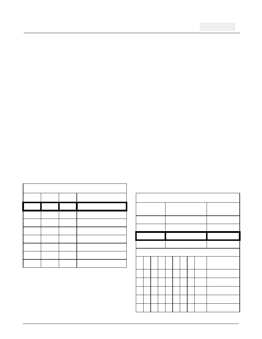
Table 5. Phase Adjust Control
Phase Adjust Input (PHASE_ADJ)
2
1
0
Phase Adjustment
0
+8.5 ps
0
1
+5.5 ps
0
1
0
+2.5 ps
0
1
0 ps
1
0
-2.5 ps
1
0
1
-5.2 ps
1
0
-8.0 ps
1
-11.0 ps
Table 6. Post-Amplifier Offset Adjust
PAOFFADJ[9:8] Settings for Resolution/Range
PAOFFADJ9
PAOFFADJ8
Resolution=
/± Range
0
0.6mV/±78mV
0
1
0.3mV/±39mV
1
0
0.22mV/±28mV
1
0.15mV/±19mV
PAOFFADJ[7:0] Settings for Offset Adjustment
7
6
5
4
3
2
1
0
α
SERDATIP-
SERDATIN =
0
-128 *
mV
0
1
-127 *
mV
0
1
0
2
-126 *
mV
0
1
3
-125 *
mV
X
α
(-128+
α)*
mV
相关PDF资料 |
PDF描述 |
|---|---|
| S1950E-FREQ-OUT25 | CRYSTAL OSCILLATOR, CLOCK, 80 MHz - 125 MHz, ACMOS OUTPUT |
| S1F78100Y2A0 | 6 V FIXED POSITIVE REGULATOR, PSSO3 |
| S1F78100Y2B0 | 5 V FIXED POSITIVE REGULATOR, PSSO3 |
| S1F78100Y2C0 | 3.2 V FIXED POSITIVE REGULATOR, PSSO3 |
| S1F78100Y2F0 | 2.2 V FIXED POSITIVE REGULATOR, PSSO3 |
相关代理商/技术参数 |
参数描述 |
|---|---|
| S19237PB13-2 | 制造商:AppliedMicro 功能描述: |
| S19237PBICC | 制造商:AppliedMicro 功能描述:IC INTERFACE TRANSCEIVER LOW POWER CMOS 255 BGA 制造商:AMCC 功能描述: |
| S19238CBI | 制造商:AppliedMicro 功能描述: |
| S19250 | 制造商:AMCC 制造商全称:Applied Micro Circuits Corporation 功能描述:STS-192 SONET/SDH/FEC/GbE/FC 16-bit Transceiver with EDC |
| S19250PBIC | 制造商:AppliedMicro 功能描述:10G SERDES EDC/SFI-4 |
发布紧急采购,3分钟左右您将得到回复。