- 您现在的位置:买卖IC网 > PDF目录192292 > S19237PB13 (APPLIEDMICRO INC) TRANSCEIVER, PBGA255 PDF资料下载
参数资料
| 型号: | S19237PB13 |
| 厂商: | APPLIEDMICRO INC |
| 元件分类: | 数字传输电路 |
| 英文描述: | TRANSCEIVER, PBGA255 |
| 封装: | PLASTIC, BGA-255 |
| 文件页数: | 44/60页 |
| 文件大小: | 1418K |
| 代理商: | S19237PB13 |
第1页第2页第3页第4页第5页第6页第7页第8页第9页第10页第11页第12页第13页第14页第15页第16页第17页第18页第19页第20页第21页第22页第23页第24页第25页第26页第27页第28页第29页第30页第31页第32页第33页第34页第35页第36页第37页第38页第39页第40页第41页第42页第43页当前第44页第45页第46页第47页第48页第49页第50页第51页第52页第53页第54页第55页第56页第57页第58页第59页第60页
S19237 – SONET STS-192/10GbE CMOS Transceiver
with ISI Compensation
AMCC Confidential and Proprietary
DS1454
49
Data Sheet
ELECTRICAL SPECIFICATIONS
Electrostatic Discharge (ESD) Sensitivity Rating - Human Body Model (HBM):
The S19237 is rated to the following ESD voltages based upon JEDEC standard: JESD22-A114-B
1. CLASS 1B - All pins are rated at or above 500 volts
Adherence to standards for ESD protection should be taken during the handling of the devices to ensure that the devices are not damaged. The
standards to be used are defined in ANSI standard ANSI/ESD S20.20-1999, “Protection of Electrical and Electronic Parts, Assemblies and
Equipment.” Contact your local FAE or sales representative for applicable ESD application notes.
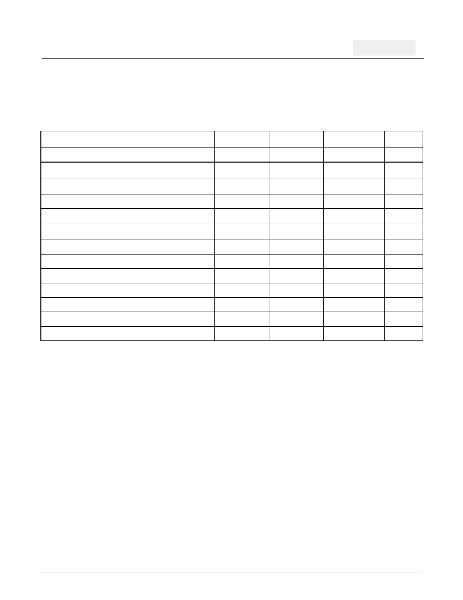
Table 23. Absolute Maximum and Minimum Ratings
The following are the absolute maximum stress ratings for the S19237 device. Stresses beyond those listed may cause permanent damage to
the device. Absolute maximum ratings are stress ratings only, and operation of the device at the maximums stated or at any other conditions
beyond those indicated in the “Recommended Operating Conditions” of the document is not inferred. Exposure to absolute maximum rating
conditions for extended periods may affect device reliability.
Parameter
Min
Typ
Max
Units
Storage temperature
-55
150
°C
VDD 1.2 V supply
1.1
1.20
1.3
V
VDD 1.8 V supply
1.65
1.80
1.95
V
VDD 1.8 V supply (when using a 3.3 V supply)
3.025
3.3
3.575
V
CML input voltage
-0.5
VDD_1.2V +0.2
V
LVCMOS control input voltage
-0.5
VDD_1.8V +0.2
V
LVDS input voltage
-0.5
VDD_1.8V +0.2
V
CML output current per pin
8
mA
CML input current per pin
8
mA
LVCMOS output current per pin
2
mA
LVCMOS input current per pin
1
mA
LVDS output current per pin
4
mA
LVDS input current per pin
2
mA
相关PDF资料 |
PDF描述 |
|---|---|
| S1950E-FREQ-OUT25 | CRYSTAL OSCILLATOR, CLOCK, 80 MHz - 125 MHz, ACMOS OUTPUT |
| S1F78100Y2A0 | 6 V FIXED POSITIVE REGULATOR, PSSO3 |
| S1F78100Y2B0 | 5 V FIXED POSITIVE REGULATOR, PSSO3 |
| S1F78100Y2C0 | 3.2 V FIXED POSITIVE REGULATOR, PSSO3 |
| S1F78100Y2F0 | 2.2 V FIXED POSITIVE REGULATOR, PSSO3 |
相关代理商/技术参数 |
参数描述 |
|---|---|
| S19237PB13-2 | 制造商:AppliedMicro 功能描述: |
| S19237PBICC | 制造商:AppliedMicro 功能描述:IC INTERFACE TRANSCEIVER LOW POWER CMOS 255 BGA 制造商:AMCC 功能描述: |
| S19238CBI | 制造商:AppliedMicro 功能描述: |
| S19250 | 制造商:AMCC 制造商全称:Applied Micro Circuits Corporation 功能描述:STS-192 SONET/SDH/FEC/GbE/FC 16-bit Transceiver with EDC |
| S19250PBIC | 制造商:AppliedMicro 功能描述:10G SERDES EDC/SFI-4 |
发布紧急采购,3分钟左右您将得到回复。