- 您现在的位置:买卖IC网 > PDF目录297338 > S29WS128J0PBFW002 (SPANSION LLC) 8M X 16 FLASH 1.8V PROM, 55 ns, PBGA84 PDF资料下载
参数资料
| 型号: | S29WS128J0PBFW002 |
| 厂商: | SPANSION LLC |
| 元件分类: | PROM |
| 英文描述: | 8M X 16 FLASH 1.8V PROM, 55 ns, PBGA84 |
| 封装: | 8 X 11.60 MM, LEAD FREE, FBGA-84 |
| 文件页数: | 21/97页 |
| 文件大小: | 2421K |
| 代理商: | S29WS128J0PBFW002 |
第1页第2页第3页第4页第5页第6页第7页第8页第9页第10页第11页第12页第13页第14页第15页第16页第17页第18页第19页第20页当前第21页第22页第23页第24页第25页第26页第27页第28页第29页第30页第31页第32页第33页第34页第35页第36页第37页第38页第39页第40页第41页第42页第43页第44页第45页第46页第47页第48页第49页第50页第51页第52页第53页第54页第55页第56页第57页第58页第59页第60页第61页第62页第63页第64页第65页第66页第67页第68页第69页第70页第71页第72页第73页第74页第75页第76页第77页第78页第79页第80页第81页第82页第83页第84页第85页第86页第87页第88页第89页第90页第91页第92页第93页第94页第95页第96页第97页
28
S29WS128J/064J
S29WS-J_00_A6 May 11, 2006
Dat a
S h ee t
10.The Password Unlock command cannot be issued any faster than 1 s at a time to prevent a
hacker from running through all the 64-bit combinations in an attempt to correctly match a
password.
11.Approximately 1 s is required for unlocking the device after the valid 64-bit password is
given to the device.
12.Password verification is only allowed during the password programming operation.
13.All further commands to the password region are disabled and all operations are ignored.
14.If the password is lost after setting the Password Mode Lock Bit, there is no way to clear the
PPB Lock Bit.
15.Entry command sequence must be issued prior to any of any operation and it disables reads
and writes for Bank 0. Reads and writes for other banks excluding Bank 0 are allowed.
16.If the user attempts to program or erase a protected sector, the device ignores the command
and returns to read mode.
17.A program or erase command to a protected sector enables status polling and returns to read
mode without having modified the contents of the protected sector.
18.The programming of the DYB, PPB, and PPB Lock for a given sector can be verified by writing
individual status read commands DYB Status, PPB Status, and PPB Lock Status to the device.
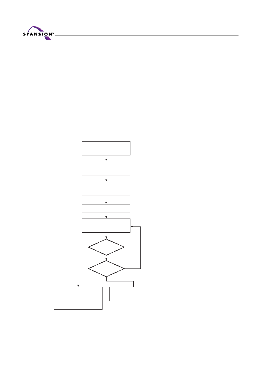
Figure 3. Lock Register Program Algorithm
Write Unlock Cycles:
Address 555h, Data AAh
Address 2AAh, Data 55h
Write
Enter Lock Register Command:
Address 555h, Data 40h
Program Lock Register Data
Address XXXh, Data A0h
Address 77h*, Data PD
Unlock Cycle 1
Unlock Cycle 2
XXXh = Address don’t care
* Not on future devices
Program Data (PD): See text for Lock Register
definitions
Caution: Lock register can only be progammed
once.
Wait 4
s
PASS. Write Lock Register
Exit Command:
Address XXXh, Data 90h
Address XXXh, Data 00h
Device returns to reading array.
Perform Polling Algorithm
(see Write Operation Status
flowchart)
Yes
No
Done?
DQ5 = 1?
Error condition (Exceeded Timing Limits)
FAIL. Write rest command
to return to reading array.
相关PDF资料 |
PDF描述 |
|---|---|
| S29WS128J0PBAW002 | 8M X 16 FLASH 1.8V PROM, 55 ns, PBGA84 |
| S2M | 2 A, 1000 V, SILICON, RECTIFIER DIODE, DO-214AA |
| S2R72A44F12C4 | UNIVERSAL SERIAL BUS CONTROLLER, PQFP48 |
| S2V20-4000 | 1.7 A, 200 V, SILICON, RECTIFIER DIODE |
| S2V60-4070 | 1.7 A, SILICON, RECTIFIER DIODE |
相关代理商/技术参数 |
参数描述 |
|---|---|
| S29WS128J0PBFW01 | 制造商:SPANSION 制造商全称:SPANSION 功能描述:128/64 Megabit (8/4 M x 16-Bit) CMOS 1.8 Volt-only Simultaneous Read/Write, Burst Mode Flash Memory |
| S29WS128J0PBFW10 | 制造商:SPANSION 制造商全称:SPANSION 功能描述:128/64 Megabit (8/4 M x 16-Bit) CMOS 1.8 Volt-only Simultaneous Read/Write, Burst Mode Flash Memory |
| S29WS128J0PBFW11 | 制造商:SPANSION 制造商全称:SPANSION 功能描述:128/64 Megabit (8/4 M x 16-Bit) CMOS 1.8 Volt-only Simultaneous Read/Write, Burst Mode Flash Memory |
| S29WS128N | 制造商:SPANSION 制造商全称:SPANSION 功能描述:256/128/64 MEGABIT CMOS 1.8 VOLT ONLY SIMULTANEOUS READ/WRITE BURST MODE FLASH MEMORY |
| S29WS128N0LBAI010 | 制造商:SPANSION 制造商全称:SPANSION 功能描述:256/128/64 MEGABIT CMOS 1.8 VOLT ONLY SIMULTANEOUS READ/WRITE BURST MODE FLASH MEMORY |
发布紧急采购,3分钟左右您将得到回复。