- 您现在的位置:买卖IC网 > PDF目录297338 > S29WS128J0PBFW002 (SPANSION LLC) 8M X 16 FLASH 1.8V PROM, 55 ns, PBGA84 PDF资料下载
参数资料
| 型号: | S29WS128J0PBFW002 |
| 厂商: | SPANSION LLC |
| 元件分类: | PROM |
| 英文描述: | 8M X 16 FLASH 1.8V PROM, 55 ns, PBGA84 |
| 封装: | 8 X 11.60 MM, LEAD FREE, FBGA-84 |
| 文件页数: | 47/97页 |
| 文件大小: | 2421K |
| 代理商: | S29WS128J0PBFW002 |
第1页第2页第3页第4页第5页第6页第7页第8页第9页第10页第11页第12页第13页第14页第15页第16页第17页第18页第19页第20页第21页第22页第23页第24页第25页第26页第27页第28页第29页第30页第31页第32页第33页第34页第35页第36页第37页第38页第39页第40页第41页第42页第43页第44页第45页第46页当前第47页第48页第49页第50页第51页第52页第53页第54页第55页第56页第57页第58页第59页第60页第61页第62页第63页第64页第65页第66页第67页第68页第69页第70页第71页第72页第73页第74页第75页第76页第77页第78页第79页第80页第81页第82页第83页第84页第85页第86页第87页第88页第89页第90页第91页第92页第93页第94页第95页第96页第97页
May 11, 2006 S29WS-J_00_A6
S29WS128J/064J
51
D a ta
Sh eet
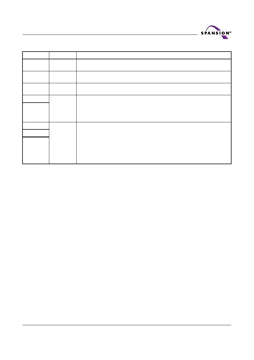
Table 17. Configuration Register
Note: Device is in the default state upon power-up or hardware reset.
Reset Command
Writing the reset command resets the banks to the read or erase-suspend-read mode. Address
bits are don’t cares for this command.
The reset command may be written between the sequence cycles in an erase command sequence
before erasing begins. This resets the bank to which the system was writing to the read mode.
Once erasure begins, however, the device ignores reset commands until the operation is
complete.
The reset command may be written between the sequence cycles in a program command se-
quence before programming begins (prior to the third cycle). This resets the bank to which the
system was writing to the read mode. If the program command sequence is written to a bank that
is in the Erase Suspend mode, writing the reset command returns that bank to the erase-sus-
pend-read mode. Once programming begins, however, the device ignores reset commands until
the operation is complete.
The reset command may be written between the sequence cycles in an autoselect command se-
quence. Once in the autoselect mode, the reset command must be written to return to the read
mode. If a bank entered the autoselect mode while in the Erase Suspend mode, writing the reset
command returns that bank to the erase-suspend-read mode.
If DQ5 goes high during a program or erase operation, writing the reset command returns the
banks to the read mode (or erase-suspend-read mode if that bank was in Erase Suspend).
Autoselect Command Sequence
The autoselect command sequence allows the host system to access the manufacturer and device
codes, and determine whether or not a sector is protected. Table 18, “Command Definitions,” on
page 60 shows the address and data requirements. The autoselect command sequence may be
Address Bit
Function
Settings (Binary)
A19
Set Device
Read Mode
0 = Synchronous Read (Burst Mode) Enabled
1 = Asynchronous Mode (default)
A18
RDY
0 = RDY active one clock cycle before data
1 = RDY active with data (default)
A17
Clock
0 = Burst starts and data is output on the falling edge of CLK
1 = Burst starts and data is output on the rising edge of CLK (default)
A16
Read Mode
Synchronous Mode
00 = Continuous (default)
01 = 8-word linear with wrap around
10 = 16-word linear with wrap around
11 = 32-word linear with wrap around
A15
A14
Programmable
Wait State
000 = Data is valid on the 2nd active CLK edge after AVD# transition to VIH
001 = Data is valid on the 3rd active CLK edge after AVD# transition to VIH
010 = Data is valid on the 4th active CLK edge after AVD# transition to VIH
011 = Data is valid on the 5th active CLK edge after AVD# transition to VIH
100 = Data is valid on the 6th active CLK edge after AVD# transition to VIH
101 = Data is valid on the 7th active CLK edge after AVD# transition to VIH (default)
110 = Reserved
111 = Reserved
A13
A12
相关PDF资料 |
PDF描述 |
|---|---|
| S29WS128J0PBAW002 | 8M X 16 FLASH 1.8V PROM, 55 ns, PBGA84 |
| S2M | 2 A, 1000 V, SILICON, RECTIFIER DIODE, DO-214AA |
| S2R72A44F12C4 | UNIVERSAL SERIAL BUS CONTROLLER, PQFP48 |
| S2V20-4000 | 1.7 A, 200 V, SILICON, RECTIFIER DIODE |
| S2V60-4070 | 1.7 A, SILICON, RECTIFIER DIODE |
相关代理商/技术参数 |
参数描述 |
|---|---|
| S29WS128J0PBFW01 | 制造商:SPANSION 制造商全称:SPANSION 功能描述:128/64 Megabit (8/4 M x 16-Bit) CMOS 1.8 Volt-only Simultaneous Read/Write, Burst Mode Flash Memory |
| S29WS128J0PBFW10 | 制造商:SPANSION 制造商全称:SPANSION 功能描述:128/64 Megabit (8/4 M x 16-Bit) CMOS 1.8 Volt-only Simultaneous Read/Write, Burst Mode Flash Memory |
| S29WS128J0PBFW11 | 制造商:SPANSION 制造商全称:SPANSION 功能描述:128/64 Megabit (8/4 M x 16-Bit) CMOS 1.8 Volt-only Simultaneous Read/Write, Burst Mode Flash Memory |
| S29WS128N | 制造商:SPANSION 制造商全称:SPANSION 功能描述:256/128/64 MEGABIT CMOS 1.8 VOLT ONLY SIMULTANEOUS READ/WRITE BURST MODE FLASH MEMORY |
| S29WS128N0LBAI010 | 制造商:SPANSION 制造商全称:SPANSION 功能描述:256/128/64 MEGABIT CMOS 1.8 VOLT ONLY SIMULTANEOUS READ/WRITE BURST MODE FLASH MEMORY |
发布紧急采购,3分钟左右您将得到回复。