- 您现在的位置:买卖IC网 > PDF目录297338 > S29WS128J0PBFW002 (SPANSION LLC) 8M X 16 FLASH 1.8V PROM, 55 ns, PBGA84 PDF资料下载
参数资料
| 型号: | S29WS128J0PBFW002 |
| 厂商: | SPANSION LLC |
| 元件分类: | PROM |
| 英文描述: | 8M X 16 FLASH 1.8V PROM, 55 ns, PBGA84 |
| 封装: | 8 X 11.60 MM, LEAD FREE, FBGA-84 |
| 文件页数: | 44/97页 |
| 文件大小: | 2421K |
| 代理商: | S29WS128J0PBFW002 |
第1页第2页第3页第4页第5页第6页第7页第8页第9页第10页第11页第12页第13页第14页第15页第16页第17页第18页第19页第20页第21页第22页第23页第24页第25页第26页第27页第28页第29页第30页第31页第32页第33页第34页第35页第36页第37页第38页第39页第40页第41页第42页第43页当前第44页第45页第46页第47页第48页第49页第50页第51页第52页第53页第54页第55页第56页第57页第58页第59页第60页第61页第62页第63页第64页第65页第66页第67页第68页第69页第70页第71页第72页第73页第74页第75页第76页第77页第78页第79页第80页第81页第82页第83页第84页第85页第86页第87页第88页第89页第90页第91页第92页第93页第94页第95页第96页第97页
May 11, 2006 S29WS-J_00_A6
S29WS128J/064J
49
D a ta
Sh eet
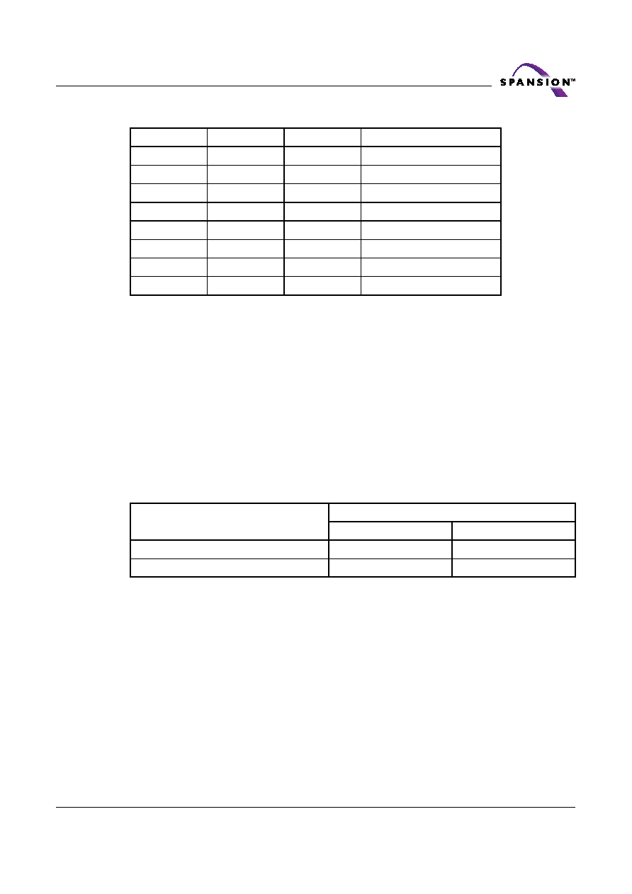
Table 14. Programmable Wait State Settings
Notes:
1. Upon power-up or hardware reset, the default setting is seven wait states.
2. RDY will default to being active with data when the Wait State Setting is set to a
total initial access cycle of 2.
It is recommended that the wait state command sequence be written, even if the default wait
state value is desired, to ensure the device is set as expected. A hardware reset will set the wait
state to the default setting.
Standard wait-state Handshaking Option
The host system must set the appropriate number of wait states in the flash device depending
upon the clock frequency. The host system should set address bits A14–A12 to 010 for a clock
frequency of 66/80 MHz for the system/device to execute at maximum speed.
Table 15 describes the recommended number of clock cycles (wait states) for various conditions.
Table 15. Wait States for Standard wait-state Handshaking
Notes:
1. In the 8-, 16- and 32-word burst read modes, the address pointer does not cross
64-word boundaries (addresses which are multiples of 3Fh).
2. For WS128J model numbers 10 and 11, an additional clock cycle is required for
boundary crossings while in Continuous read mode.
The host system must set the appropriate number of wait states in the flash device depending
upon the clock frequency. Note that the host system must set again the number of wait state
when the host system change the clock frequency. For example, the host system must set from
6 or 7 wait state to less than 5 wait states when the host system change the clock frequency from
80MHz to less than 80MHz. The autoselect function allows the host system to determine whether
the flash device is enabled for handshaking. See the “Autoselect Command Sequence” section on
page 51 for more information.
A14
A13
A12
Total Initial Access Cycles
0
2
0
1
3
0
1
0
4
0
1
5
1
0
6
1
0
1
7 (default)
1
0
Reserved
1
Reserved
Burst Mode
Typical No. of Clock Cycles after AVD# Low
66 MHz
80 MHz
8-Word or 16-Word or Continuous
4
6 or 7
32-Word
5
7
相关PDF资料 |
PDF描述 |
|---|---|
| S29WS128J0PBAW002 | 8M X 16 FLASH 1.8V PROM, 55 ns, PBGA84 |
| S2M | 2 A, 1000 V, SILICON, RECTIFIER DIODE, DO-214AA |
| S2R72A44F12C4 | UNIVERSAL SERIAL BUS CONTROLLER, PQFP48 |
| S2V20-4000 | 1.7 A, 200 V, SILICON, RECTIFIER DIODE |
| S2V60-4070 | 1.7 A, SILICON, RECTIFIER DIODE |
相关代理商/技术参数 |
参数描述 |
|---|---|
| S29WS128J0PBFW01 | 制造商:SPANSION 制造商全称:SPANSION 功能描述:128/64 Megabit (8/4 M x 16-Bit) CMOS 1.8 Volt-only Simultaneous Read/Write, Burst Mode Flash Memory |
| S29WS128J0PBFW10 | 制造商:SPANSION 制造商全称:SPANSION 功能描述:128/64 Megabit (8/4 M x 16-Bit) CMOS 1.8 Volt-only Simultaneous Read/Write, Burst Mode Flash Memory |
| S29WS128J0PBFW11 | 制造商:SPANSION 制造商全称:SPANSION 功能描述:128/64 Megabit (8/4 M x 16-Bit) CMOS 1.8 Volt-only Simultaneous Read/Write, Burst Mode Flash Memory |
| S29WS128N | 制造商:SPANSION 制造商全称:SPANSION 功能描述:256/128/64 MEGABIT CMOS 1.8 VOLT ONLY SIMULTANEOUS READ/WRITE BURST MODE FLASH MEMORY |
| S29WS128N0LBAI010 | 制造商:SPANSION 制造商全称:SPANSION 功能描述:256/128/64 MEGABIT CMOS 1.8 VOLT ONLY SIMULTANEOUS READ/WRITE BURST MODE FLASH MEMORY |
发布紧急采购,3分钟左右您将得到回复。