- 您现在的位置:买卖IC网 > PDF目录297338 > S29WS128J0PBFW002 (SPANSION LLC) 8M X 16 FLASH 1.8V PROM, 55 ns, PBGA84 PDF资料下载
参数资料
| 型号: | S29WS128J0PBFW002 |
| 厂商: | SPANSION LLC |
| 元件分类: | PROM |
| 英文描述: | 8M X 16 FLASH 1.8V PROM, 55 ns, PBGA84 |
| 封装: | 8 X 11.60 MM, LEAD FREE, FBGA-84 |
| 文件页数: | 50/97页 |
| 文件大小: | 2421K |
| 代理商: | S29WS128J0PBFW002 |
第1页第2页第3页第4页第5页第6页第7页第8页第9页第10页第11页第12页第13页第14页第15页第16页第17页第18页第19页第20页第21页第22页第23页第24页第25页第26页第27页第28页第29页第30页第31页第32页第33页第34页第35页第36页第37页第38页第39页第40页第41页第42页第43页第44页第45页第46页第47页第48页第49页当前第50页第51页第52页第53页第54页第55页第56页第57页第58页第59页第60页第61页第62页第63页第64页第65页第66页第67页第68页第69页第70页第71页第72页第73页第74页第75页第76页第77页第78页第79页第80页第81页第82页第83页第84页第85页第86页第87页第88页第89页第90页第91页第92页第93页第94页第95页第96页第97页
54
S29WS128J/064J
S29WS-J_00_A6 May 11, 2006
Dat a
S h ee t
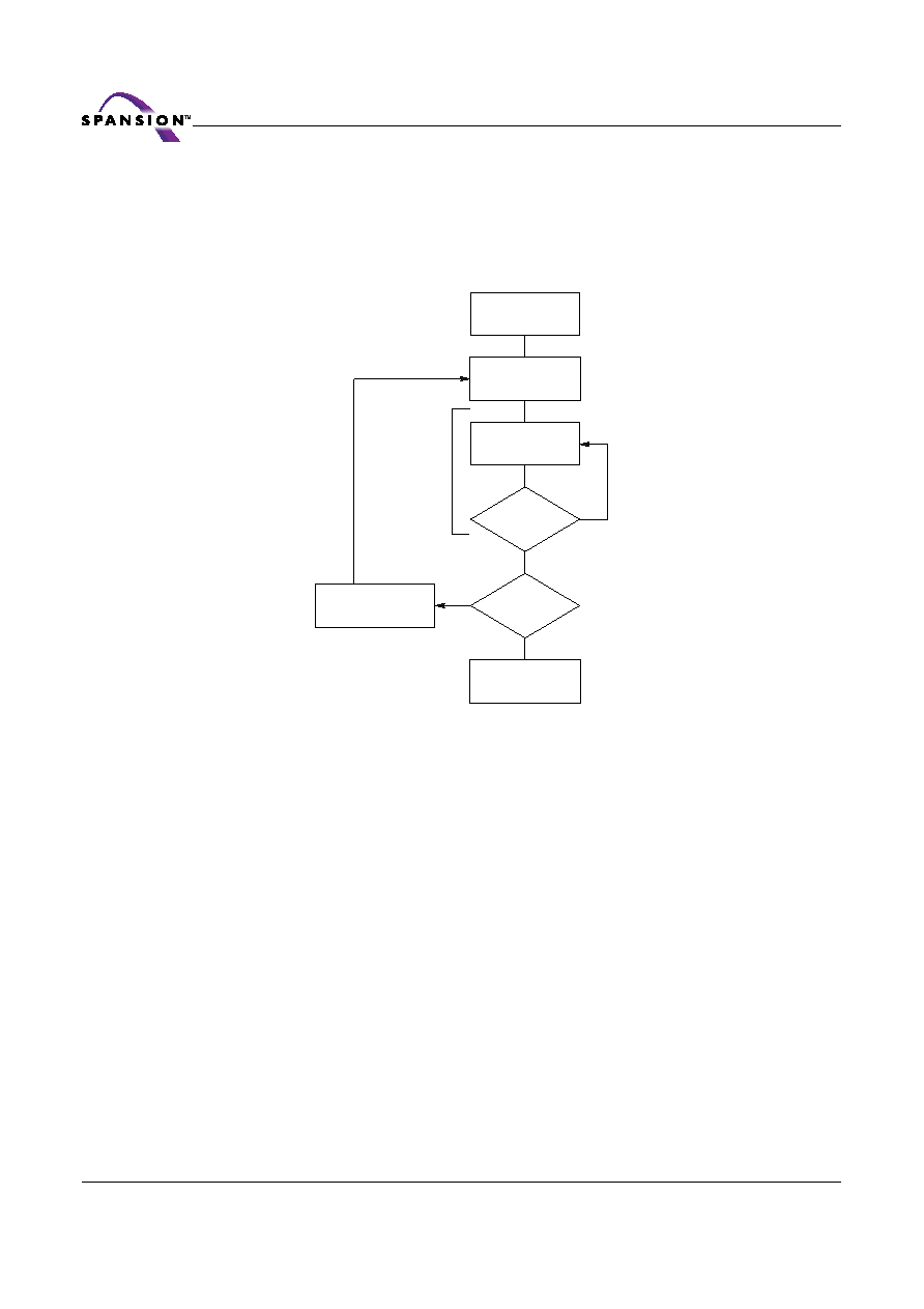
Figure 5, “Program Operation,” on page 54 illustrates the algorithm for the program operation.
Refer to the Erase/Program Operations table in the AC Characteristics section for parameters, and
for timing diagrams.
Note: See Table 18 for program command sequence.
Figure 5. Program Operation
Chip Erase Command Sequence
Chip erase is a six bus cycle operation. The chip erase command sequence is initiated by writing
two unlock cycles, followed by a set-up command. Two additional unlock write cycles are then
followed by the chip erase command, which in turn invokes the Embedded Erase algorithm. The
device does not require the system to preprogram prior to erase. The Embedded Erase algorithm
automatically preprograms and verifies the entire memory for an all zero data pattern prior to
electrical erase. The system is not required to provide any controls or timings during these oper-
ations. Table 18, “Command Definitions,” on page 60 shows the address and data requirements
for the chip erase command sequence.
When the Embedded Erase algorithm is complete, that bank returns to the read mode and ad-
dresses are no longer latched. The system can determine the status of the erase operation by
using DQ7 or DQ6/DQ2. Refer to the “Write Operation Status” section on page 62 for information
on these status bits.
Any commands written during the chip erase operation are ignored. However, note that a hard-
ware reset immediately terminates the erase operation. If that occurs, the chip erase command
sequence should be reinitiated once that bank has returned to reading array data, to ensure data
integrity.
START
Write Program
Command Sequence
Data Poll
from System
Verify Data?
No
Yes
Last Address?
No
Yes
Programming
Completed
Increment Address
Embedded
Program
algorithm
in progress
相关PDF资料 |
PDF描述 |
|---|---|
| S29WS128J0PBAW002 | 8M X 16 FLASH 1.8V PROM, 55 ns, PBGA84 |
| S2M | 2 A, 1000 V, SILICON, RECTIFIER DIODE, DO-214AA |
| S2R72A44F12C4 | UNIVERSAL SERIAL BUS CONTROLLER, PQFP48 |
| S2V20-4000 | 1.7 A, 200 V, SILICON, RECTIFIER DIODE |
| S2V60-4070 | 1.7 A, SILICON, RECTIFIER DIODE |
相关代理商/技术参数 |
参数描述 |
|---|---|
| S29WS128J0PBFW01 | 制造商:SPANSION 制造商全称:SPANSION 功能描述:128/64 Megabit (8/4 M x 16-Bit) CMOS 1.8 Volt-only Simultaneous Read/Write, Burst Mode Flash Memory |
| S29WS128J0PBFW10 | 制造商:SPANSION 制造商全称:SPANSION 功能描述:128/64 Megabit (8/4 M x 16-Bit) CMOS 1.8 Volt-only Simultaneous Read/Write, Burst Mode Flash Memory |
| S29WS128J0PBFW11 | 制造商:SPANSION 制造商全称:SPANSION 功能描述:128/64 Megabit (8/4 M x 16-Bit) CMOS 1.8 Volt-only Simultaneous Read/Write, Burst Mode Flash Memory |
| S29WS128N | 制造商:SPANSION 制造商全称:SPANSION 功能描述:256/128/64 MEGABIT CMOS 1.8 VOLT ONLY SIMULTANEOUS READ/WRITE BURST MODE FLASH MEMORY |
| S29WS128N0LBAI010 | 制造商:SPANSION 制造商全称:SPANSION 功能描述:256/128/64 MEGABIT CMOS 1.8 VOLT ONLY SIMULTANEOUS READ/WRITE BURST MODE FLASH MEMORY |
发布紧急采购,3分钟左右您将得到回复。