- 您现在的位置:买卖IC网 > PDF目录297338 > S29WS128J0PBFW002 (SPANSION LLC) 8M X 16 FLASH 1.8V PROM, 55 ns, PBGA84 PDF资料下载
参数资料
| 型号: | S29WS128J0PBFW002 |
| 厂商: | SPANSION LLC |
| 元件分类: | PROM |
| 英文描述: | 8M X 16 FLASH 1.8V PROM, 55 ns, PBGA84 |
| 封装: | 8 X 11.60 MM, LEAD FREE, FBGA-84 |
| 文件页数: | 46/97页 |
| 文件大小: | 2421K |
| 代理商: | S29WS128J0PBFW002 |
第1页第2页第3页第4页第5页第6页第7页第8页第9页第10页第11页第12页第13页第14页第15页第16页第17页第18页第19页第20页第21页第22页第23页第24页第25页第26页第27页第28页第29页第30页第31页第32页第33页第34页第35页第36页第37页第38页第39页第40页第41页第42页第43页第44页第45页当前第46页第47页第48页第49页第50页第51页第52页第53页第54页第55页第56页第57页第58页第59页第60页第61页第62页第63页第64页第65页第66页第67页第68页第69页第70页第71页第72页第73页第74页第75页第76页第77页第78页第79页第80页第81页第82页第83页第84页第85页第86页第87页第88页第89页第90页第91页第92页第93页第94页第95页第96页第97页
50
S29WS128J/064J
S29WS-J_00_A6 May 11, 2006
Dat a
S h ee t
Read Mode Configuration
The device supports four different read modes: continuous mode, and 8, 16, and 32 word linear
wrap around modes. A continuous sequence begins at the starting address and advances the ad-
dress pointer until the burst operation is complete. If the highest address in the device is reached
during the continuous burst read mode, the address pointer wraps around to the lowest address.
For example, an eight-word linear read with wrap around begins on the starting address written
to the device and then advances to the next 8 word boundary. The address pointer then returns
to the 1st word after the previous eight word boundary, wrapping through the starting location.
The sixteen- and thirty-two linear wrap around modes operate in a fashion similar to the eight-
word mode.
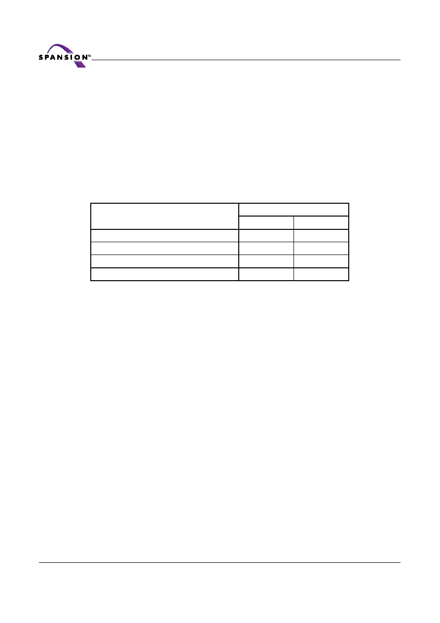
Table 16 shows the address bits and settings for the four read modes.
Table 16. Read Mode Settings
Note: Upon power-up or hardware reset the default setting is continuous.
Burst Active Clock Edge Configuration
By default, the device will deliver data on the rising edge of the clock after the initial synchronous
access time. Subsequent outputs will also be on the following rising edges, barring any delays.
The device can be set so that the falling clock edge is active for all synchronous accesses. Address
bit A17 determines this setting; “1” for rising active, “0” for falling active.
RDY Configuration
By default, the device is set so that the RDY pin will output VOH whenever there is valid data on
the outputs. The device can be set so that RDY goes active one data cycle before active data.
Address bit A18 determines this setting; “1” for RDY active with data, “0” for RDY active one clock
cycle before valid data. Only the combination of wait state 2 and RDY active one clock cycle before
data is not supported. In asynchronous mode, RDY is an open-drain output.
Configuration Register
Table 17 shows the address bits that determine the configuration register settings for various de-
vice functions.
Burst Modes
Address Bits
A16
A15
Continuous
0
8-word linear wrap around
0
1
16-word linear wrap around
1
0
32-word linear wrap around
1
相关PDF资料 |
PDF描述 |
|---|---|
| S29WS128J0PBAW002 | 8M X 16 FLASH 1.8V PROM, 55 ns, PBGA84 |
| S2M | 2 A, 1000 V, SILICON, RECTIFIER DIODE, DO-214AA |
| S2R72A44F12C4 | UNIVERSAL SERIAL BUS CONTROLLER, PQFP48 |
| S2V20-4000 | 1.7 A, 200 V, SILICON, RECTIFIER DIODE |
| S2V60-4070 | 1.7 A, SILICON, RECTIFIER DIODE |
相关代理商/技术参数 |
参数描述 |
|---|---|
| S29WS128J0PBFW01 | 制造商:SPANSION 制造商全称:SPANSION 功能描述:128/64 Megabit (8/4 M x 16-Bit) CMOS 1.8 Volt-only Simultaneous Read/Write, Burst Mode Flash Memory |
| S29WS128J0PBFW10 | 制造商:SPANSION 制造商全称:SPANSION 功能描述:128/64 Megabit (8/4 M x 16-Bit) CMOS 1.8 Volt-only Simultaneous Read/Write, Burst Mode Flash Memory |
| S29WS128J0PBFW11 | 制造商:SPANSION 制造商全称:SPANSION 功能描述:128/64 Megabit (8/4 M x 16-Bit) CMOS 1.8 Volt-only Simultaneous Read/Write, Burst Mode Flash Memory |
| S29WS128N | 制造商:SPANSION 制造商全称:SPANSION 功能描述:256/128/64 MEGABIT CMOS 1.8 VOLT ONLY SIMULTANEOUS READ/WRITE BURST MODE FLASH MEMORY |
| S29WS128N0LBAI010 | 制造商:SPANSION 制造商全称:SPANSION 功能描述:256/128/64 MEGABIT CMOS 1.8 VOLT ONLY SIMULTANEOUS READ/WRITE BURST MODE FLASH MEMORY |
发布紧急采购,3分钟左右您将得到回复。