- 您现在的位置:买卖IC网 > PDF目录297338 > S29WS128J0PBFW002 (SPANSION LLC) 8M X 16 FLASH 1.8V PROM, 55 ns, PBGA84 PDF资料下载
参数资料
| 型号: | S29WS128J0PBFW002 |
| 厂商: | SPANSION LLC |
| 元件分类: | PROM |
| 英文描述: | 8M X 16 FLASH 1.8V PROM, 55 ns, PBGA84 |
| 封装: | 8 X 11.60 MM, LEAD FREE, FBGA-84 |
| 文件页数: | 58/97页 |
| 文件大小: | 2421K |
| 代理商: | S29WS128J0PBFW002 |
第1页第2页第3页第4页第5页第6页第7页第8页第9页第10页第11页第12页第13页第14页第15页第16页第17页第18页第19页第20页第21页第22页第23页第24页第25页第26页第27页第28页第29页第30页第31页第32页第33页第34页第35页第36页第37页第38页第39页第40页第41页第42页第43页第44页第45页第46页第47页第48页第49页第50页第51页第52页第53页第54页第55页第56页第57页当前第58页第59页第60页第61页第62页第63页第64页第65页第66页第67页第68页第69页第70页第71页第72页第73页第74页第75页第76页第77页第78页第79页第80页第81页第82页第83页第84页第85页第86页第87页第88页第89页第90页第91页第92页第93页第94页第95页第96页第97页
May 11, 2006 S29WS-J_00_A6
S29WS128J/064J
61
D a ta
Sh eet
Legend:
X = Don’t care
RA = Address of the memory location to be read.
RD = Data read from location RA during read operation.
PA = Address of the memory location to be programmed. Addresses latch on the rising edge of the AVD# pulse or active edge of CLK which ever
comes first.
PD = Data to be programmed at location PA. Data latches on the rising edge of WE# or CE# pulse, whichever happens first.
SA = Address of the sector to be verified (in autoselect mode) or erased. Address bits Amax–A12 uniquely select any sector.
BA = Address of the bank (WS128J: A22, A21, A20, WS064J: A21, A20, A19) that is being switched to autoselect mode, is in bypass mode, or is
being erased.
SLA = Address of the sector to be locked. Set sector address (SA) and either A6 = 1 for unlocked or A6 = 0 for locked.
SBA = sector address block to be protected.
CR = Configuration Register address bits A19–A12.
OW = Address (A7–A0) is (00011010).
PD3–PD0 = Password Data. PD3–PD0 present four 16 bit combinations that represent the 64-bit Password
PWA = Password Address. Address bits A1 and A0 are used to select each 16-bit portion of the 64-bit entity.
PWD = Password Data.
PL = Address (A7-A0) is (00001010)
RD(0) = DQ0 protection indicator bit. If protected, DQ0 = 1, if unprotected, DQ0 = 0.
RD(1) = DQ1 protection indicator bit. If protected, DQ1 = 1, if unprotected, DQ1 = 0.
SL = Address (A7-A0) is (00010010)
WD= Write Data. See “Configuration Register” definition for specific write data
WP = Address (A7-A0) is (00000010)
WPE = address(A7-A0) is (01000010)
Notes:
1. See Table 1 for description of bus operations.
2. All values are in hexadecimal.
3. Except for the following, all bus cycles are write cycle: read cycle, fourth through sixth cycles of the Autoselect commands, fourth cycle of
the configuration register verify and password verify commands, and any cycle reading at RD(0) and RD(1).
4. Data bits DQ15–DQ8 are don’t care in command sequences, except for RD, PD, WD, PWD, and PD3-PD0.
5. Unless otherwise noted, address bits Amax–A12 are don’t cares.
6. Writing incorrect address and data values or writing them in the improper sequence may place the device in an unknown state. The system
must write the reset command to return the device to reading array data.
7. No unlock or command cycles required when bank is reading array data.
8. The Reset command is required to return to reading array data (or to the erase-suspend-read mode if previously in Erase Suspend) when a
bank is in the autoselect mode, or if DQ5 goes high (while the bank is providing status information) or performing sector lock/unlock.
9. The fourth cycle of the autoselect command sequence is a read cycle. The system must provide the bank address. See the Autoselect
Command Sequence section for more information.
10. (BA)X0Fh = 2200h (WS128J), (BA)X0Eh = 2218h (WS128J), (BA)X0Fh = 221Eh (WS064J), (BA)X0Eh = 2201h (WS064J)
11. The data is 0000h for an unlocked sector and 0001h for a locked sector
12. DQ15 - DQ8 = 0, DQ7 - Factory Lock Bit (1 = Locked, 0 = Not Locked), DQ6 -Customer Lock Bit (1 = Locked, 0 = Not Locked), DQ5 =
Handshake Bit (1 = Reserved, 0 = Standard Handshake)8, DQ4 & DQ3 - Boot Code (00= Dual Boot Sector, 01= Top Boot Sector, 10=
Bottom Boot Sector, 11=No Boot Sector), DQ2 - DQ0 = 001
13. The Unlock Bypass command sequence is required prior to this command sequence.
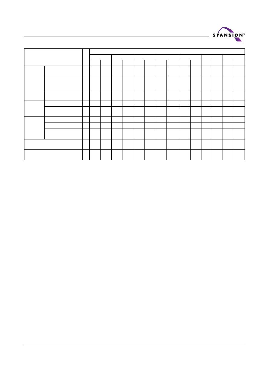
PPB
Commands
PPB Program (Notes
6
555
AA
2AA
55
555
60
SBA
+ WP
68
SBA
+ WP
48
XX
RD
(0)
All PPB Erase (Notes
6
555
AA
2AA
55
555
60
WPE
60
SBA
WPE
40
XX
RD
(0)
PPB Status (Note 25) 4
555
AA
2AA
55
SBA
555
90
SBA
+WP
RD
(0)
PPB Lock
Bit
PPB Lock Bit Set
3
555
AA
2AA
55
555
78
PPB Lock Bit Status
4
555
AA
2AA
55
(BA)
555
58
BA
RD
(1)
DPB
DPB Write
4
555
AA
2AA
55
555
48
SA
X1
DPB Erase
4
555
AA
2AA
55
555
48
SA
X0
DPB Status
4
555
AA
2AA
55
(BA)
555
58
SA
RD
(0)
Password Protection Mode
Locking Bit Program (Notes 21)
6
555
AA
2AA
55
555
60
PL
68
PL
48
PL
RD
(0)
Persistent Protection Mode
Locking Bit Program (Notes 21)
6
555
AA
2AA
55
555
60
SL
68
SL
48
SL
RD
(0)
Command Sequence
(Note 1)
Cy
cl
es
Bus Cycles (Notes 1–6)
First
Second
Third
Fourth
Fifth
Sixth
Seventh
Addr
Data
Addr
Data
Addr
Data
Addr
Data
Addr
Data
Addr
Data
Addr
Data
相关PDF资料 |
PDF描述 |
|---|---|
| S29WS128J0PBAW002 | 8M X 16 FLASH 1.8V PROM, 55 ns, PBGA84 |
| S2M | 2 A, 1000 V, SILICON, RECTIFIER DIODE, DO-214AA |
| S2R72A44F12C4 | UNIVERSAL SERIAL BUS CONTROLLER, PQFP48 |
| S2V20-4000 | 1.7 A, 200 V, SILICON, RECTIFIER DIODE |
| S2V60-4070 | 1.7 A, SILICON, RECTIFIER DIODE |
相关代理商/技术参数 |
参数描述 |
|---|---|
| S29WS128J0PBFW01 | 制造商:SPANSION 制造商全称:SPANSION 功能描述:128/64 Megabit (8/4 M x 16-Bit) CMOS 1.8 Volt-only Simultaneous Read/Write, Burst Mode Flash Memory |
| S29WS128J0PBFW10 | 制造商:SPANSION 制造商全称:SPANSION 功能描述:128/64 Megabit (8/4 M x 16-Bit) CMOS 1.8 Volt-only Simultaneous Read/Write, Burst Mode Flash Memory |
| S29WS128J0PBFW11 | 制造商:SPANSION 制造商全称:SPANSION 功能描述:128/64 Megabit (8/4 M x 16-Bit) CMOS 1.8 Volt-only Simultaneous Read/Write, Burst Mode Flash Memory |
| S29WS128N | 制造商:SPANSION 制造商全称:SPANSION 功能描述:256/128/64 MEGABIT CMOS 1.8 VOLT ONLY SIMULTANEOUS READ/WRITE BURST MODE FLASH MEMORY |
| S29WS128N0LBAI010 | 制造商:SPANSION 制造商全称:SPANSION 功能描述:256/128/64 MEGABIT CMOS 1.8 VOLT ONLY SIMULTANEOUS READ/WRITE BURST MODE FLASH MEMORY |
发布紧急采购,3分钟左右您将得到回复。