- 您现在的位置:买卖IC网 > Datasheet目录369 > W9725G6KB-25I (Winbond Electronics)IC DDR2 SDRAM 256MBIT 84WBGA Datasheet资料下载
参数资料
| 型号: | W9725G6KB-25I |
| 厂商: | Winbond Electronics |
| 文件页数: | 20/87页 |
| 文件大小: | 0K |
| 描述: | IC DDR2 SDRAM 256MBIT 84WBGA |
| 标准包装: | 209 |
| 格式 - 存储器: | RAM |
| 存储器类型: | DDR2 SDRAM |
| 存储容量: | 256M(16Mx16) |
| 速度: | 2.5ns |
| 接口: | 并联 |
| 电源电压: | 1.7 V ~ 1.9 V |
| 工作温度: | -40°C ~ 95°C |
| 封装/外壳: | 84-TFBGA |
| 供应商设备封装: | 84-WBGA(8x12.5) |
| 包装: | * |
| 其它名称: | Q7118748 |
第1页第2页第3页第4页第5页第6页第7页第8页第9页第10页第11页第12页第13页第14页第15页第16页第17页第18页第19页当前第20页第21页第22页第23页第24页第25页第26页第27页第28页第29页第30页第31页第32页第33页第34页第35页第36页第37页第38页第39页第40页第41页第42页第43页第44页第45页第46页第47页第48页第49页第50页第51页第52页第53页第54页第55页第56页第57页第58页第59页第60页第61页第62页第63页第64页第65页第66页第67页第68页第69页第70页第71页第72页第73页第74页第75页第76页第77页第78页第79页第80页第81页第82页第83页第84页第85页第86页第87页
�� �
�
�W9725G6KB�
�8.3�
�8.3.1�
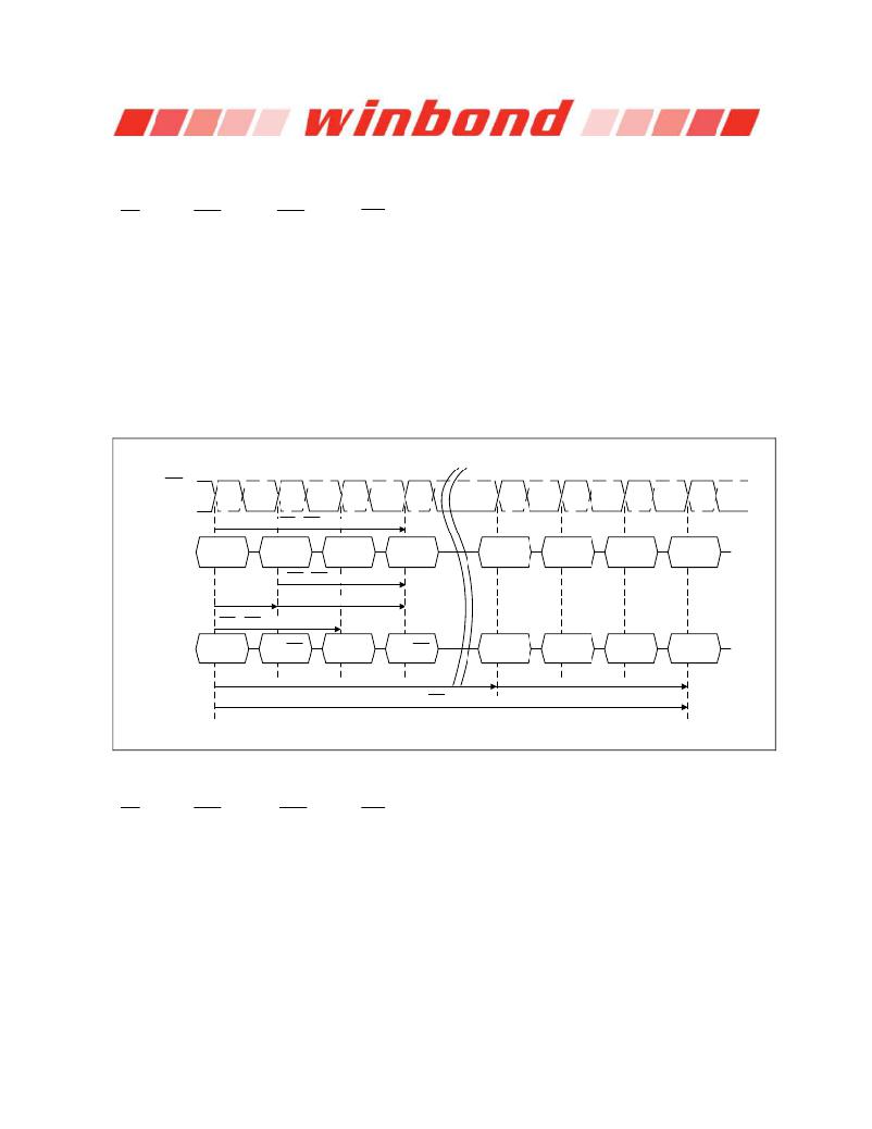
�Command� Function�
�Bank� Activate� Command�
�(� CS� =� "L",� RAS� =� "L",� CAS� =� "H",� WE� =� "H",� BA0,� BA1� =� Bank,� A0� to� A12� be� row� address)�
�The� Bank� Activate� command� must� be� applied� before� any� Read� or� Write� operation� can� be� executed.�
�Immediately� after� the� bank� active� command,� the� DDR2� SDRAM� can� accept� a� read� or� write� command�
�on� the� following� clock� cycle.� If� a� Read/Write� command� is� issued� to� a� bank� that� has� not� satisfied� the�
�t� RCDmin� specification,� then� additive� latency� must� be� programmed� into� the� device� to� delay� when� the�
�Read/Write� command� is� internally� issued� to� the� device.� The� additive� latency� value� must� be� chosen� to�
�assure� t� RCDmin� is� satisfied.� Additive� latencies� of� 0,� 1,� 2,� 3,� 4,� 5� and� 6� are� supported.� Once� a� bank� has�
�been� activated� it� must� be� precharged� before� another� Bank� Activate� command� can� be� applied� to� the�
�same� bank.� The� bank� active� and� precharge� times� are� defined� as� t� RAS� and� t� RP� ,� respectively.� The�
�minimum� time� interval� between� successive� Bank� Activate� commands� to� the� same� bank� is� determined�
�by� the� RAS� cycle� time� of� the� device� (t� RC� ).� The� minimum� time� interval� between� Bank� Activate�
�commands� is� t� RRD� .�
�T0�
�T1�
�T2�
�T3�
�Tn�
�Tn+1�
�Tn+2�
�Tn+3�
�CLK�
�CLK�
�Internal� RAS� -� RAS� delay� (� ≥� t� RCD� min)�
�Address�
�Bank� A�
�Row� Addr.�
�Bank� A�
�Col.� Addr.�
�Bank� B�
�Row� Addr.�
�Bank� B�
�Col.� Addr.�
�Bank� A�
�Addr.�
�Bank� B�
�Addr.�
�Bank� A�
�Row� Addr.�
�CAS - CAS delay time(t� CCD� )�
�t� RCD� =� 1�
�Additive Latency delay(AL)�
�Read� Begins�
�RAS - RAS delay time(≥ t� RRD� )�
�Command�
�Bank� A�
�Activate�
�Bank� A�
�Post� CAS�
�Read�
�Bank� B�
�Activate�
�Bank� B�
�Post� CAS�
�Read�
�Bank� A�
�Precharge�
�Bank� B�
�Precharge�
�Bank� A�
�Activate�
�Bank� Active� (� ≥� t� RAS� )�
�Bank� Precharge� time� (� ≥� t� RP� )�
�RAS Cycle time (≥ t� RC� )�
�Figure� 12� –� Bank� activate� command� cycle:� t� RCD� =� 3,� AL� =� 2,� t� RP� =� 3,� t� RRD� =� 2,� t� CCD� =� 2�
�8.3.2�
�Read� Command�
�(� CS� =� "L",� RAS� =� "H",� CAS� =� "L",� WE� =� "H",� BA0,� BA1� =� Bank,� A10� =� "L",� A0� to� A8� =� Column�
�Address)�
�The� READ� command� is� used� to� initiate� a� burst� read� access� to� an� active� row.� The� value� on� BA0,� BA1�
�inputs� selects� the� bank,� and� the� A0� to� A8� address� inputs� determine� the� starting� column� address.� The�
�address� input� A10� determines� whether� or� not� Auto-precharge� is� used.� If� Auto-precharge� is� selected,�
�the� row� being� accessed� will� be� precharged� at� the� end� of� the� READ� burst;� if� Auto-precharge� is� not�
�selected,� the� row� will� remain� open� for� subsequent� accesses.�
�Publication� Release� Date:� Sep.� 03,� 2012�
�-� 20� -�
�Revision� A03�
�相关PDF资料 |
PDF描述 |
|---|---|
| W972GG6JB-3I | IC DDR2 SDRAM 2GBITS 84WBGA |
| W9751G6IB-25 | IC DDR2-800 SDRAM 512MB 84-WBGA |
| W9751G6KB-25 | IC DDR2 SDRAM 512MBIT 84WBGA |
| W9812G6JH-6I | IC SDRAM 128MBIT 54TSOPII |
| W9816G6IH-6I | IC SDRAM 16MBIT 50TSOPII |
相关代理商/技术参数 |
参数描述 |
|---|---|
| W9725G6KB25I TR | 制造商:Winbond Electronics Corp 功能描述:256M DDR2-800, X16, IND TEMP |
| W9725G6KB25K | 制造商:WINBOND 制造商全称:Winbond 功能描述:DLL aligns DQ and DQS transitions with clock, Data masks (DM) for write data, Write Data Mask |
| W9725G6KB-3 | 制造商:WINBOND 制造商全称:Winbond 功能描述:DLL aligns DQ and DQS transitions with clock, Data masks (DM) for write data, Write Data Mask |
| W9725G8JB | 制造商:WINBOND 制造商全称:Winbond 功能描述:8M ? 4 BANKS ? 8 BIT DDR2 SDRAM |
| W9725G8JB25 | 制造商:Winbond Electronics Corp 功能描述:DRAM Chip DDR2 SDRAM 256M-Bit 32Mx8 1.8V 60-Pin WBGA |
发布紧急采购,3分钟左右您将得到回复。