参数资料
| 型号: | ADV7184BSTZ |
| 厂商: | Analog Devices Inc |
| 文件页数: | 92/112页 |
| 文件大小: | 0K |
| 描述: | IC DECODER VID SDTV MULTI 80LQFP |
| 标准包装: | 1 |
| 类型: | 视频解码器 |
| 应用: | 投影仪,录音机,安全 |
| 电压 - 电源,模拟: | 3.15 V ~ 3.45 V |
| 电压 - 电源,数字: | 1.65 V ~ 2 V |
| 安装类型: | 表面贴装 |
| 封装/外壳: | 80-LQFP |
| 供应商设备封装: | 80-LQFP(14x14) |
| 包装: | 托盘 |
第1页第2页第3页第4页第5页第6页第7页第8页第9页第10页第11页第12页第13页第14页第15页第16页第17页第18页第19页第20页第21页第22页第23页第24页第25页第26页第27页第28页第29页第30页第31页第32页第33页第34页第35页第36页第37页第38页第39页第40页第41页第42页第43页第44页第45页第46页第47页第48页第49页第50页第51页第52页第53页第54页第55页第56页第57页第58页第59页第60页第61页第62页第63页第64页第65页第66页第67页第68页第69页第70页第71页第72页第73页第74页第75页第76页第77页第78页第79页第80页第81页第82页第83页第84页第85页第86页第87页第88页第89页第90页第91页当前第92页第93页第94页第95页第96页第97页第98页第99页第100页第101页第102页第103页第104页第105页第106页第107页第108页第109页第110页第111页第112页
ADV7184
Rev. A | Page 80 of 112
MPU PORT DESCRIPTION
The ADV7184 supports a 2-wire (I2C-compatible) serial inter-
face. Two inputs, serial data (SDA) and serial clock (SCLK),
carry information between the ADV7184 and the system I2C
master controller. Each slave device is recognized by a unique
address. The ADV7184 I2C port allows the user to set up and
configure the decoder and then to read back captured VBI data.
The ADV7184 has two possible slave addresses for both read
and write operations, depending on the logic level on the ALSB
pin. These four unique addresses are shown in Table 103. The
ADV7184 ALSB pin controls Bit 1 of the slave address. By
altering the ALSB, it is possible to control two ADV7184s in an
application without having a conflict with the same slave
address. The LSB (Bit 0) sets either a read or write operation.
Logic 1 corresponds to a read operation; Logic 0 corresponds to
a write operation.
Table 103. I2C Address
ALSB
R/W
Slave Address
0
0x40
0
1
0x41
1
0
0x42
1
0x43
To control the device on the bus, a specific protocol must be
followed. First, the master initiates a data transfer by establishing a
start condition, which is defined by a high-to-low transition on
SDA while SCLK remains high. This indicates that an address/data
stream follows. All peripherals respond to the start condition
and shift the next eight bits (7-bit address + R/W bit). The bits
are transferred from MSB down to LSB. The peripheral that
recognizes the transmitted address responds by pulling the
data line low during the ninth clock pulse; this is known as an
acknowledge bit. All other devices withdraw from the bus at
this point and maintain an idle condition. The idle condition is
where the device monitors the SDA and SCLK lines, waiting for
the start condition and the correct transmitted address.
The R/W bit determines the direction of the data. If the first
byte of the LSB is Logic 0, the master writes information to the
peripheral. If the first byte of the LSB is Logic 1, the master reads
information from the peripheral.
The ADV7184 acts as a standard slave device on the bus. The
data on the SDA pin is eight bits long, supporting the 7-bit
addresses plus the R/W bit. The ADV7184 has 249 subaddresses
to enable access to the internal registers. It therefore interprets
the first byte as the device address and the second byte as the
starting subaddress. The subaddresses autoincrement, allowing
data to be written to or read from the starting subaddress. A
data transfer is always terminated by a stop condition. The user
can also access any subaddress register on a one-by-one basis
without updating all the registers.
Stop and start conditions can be detected at any stage during the
data transfer. If these conditions are asserted out of sequence with
normal read and write operations, they cause an immediate
jump to the idle condition. During a given SCLK high period,
the user should issue only one start condition, one stop condition,
or a single stop condition followed by a single start condition. If
an invalid subaddress is issued by the user, the ADV7184 does
not issue an acknowledge and returns to the idle condition.
If the highest subaddress is exceeded in autoincrement mode,
the following action is taken:
1.
During a read, the highest subaddress register contents
continue to be output until the master device issues a no
acknowledge. This indicates the end of a read. In a no
acknowledge condition, the SDA line is not pulled low on
the ninth pulse.
2.
During a write, the data for the invalid byte is not loaded into
a subaddress register. Instead, a no acknowledge is issued
by the ADV7184, and the part returns to the idle condition.
05
47
9-
049
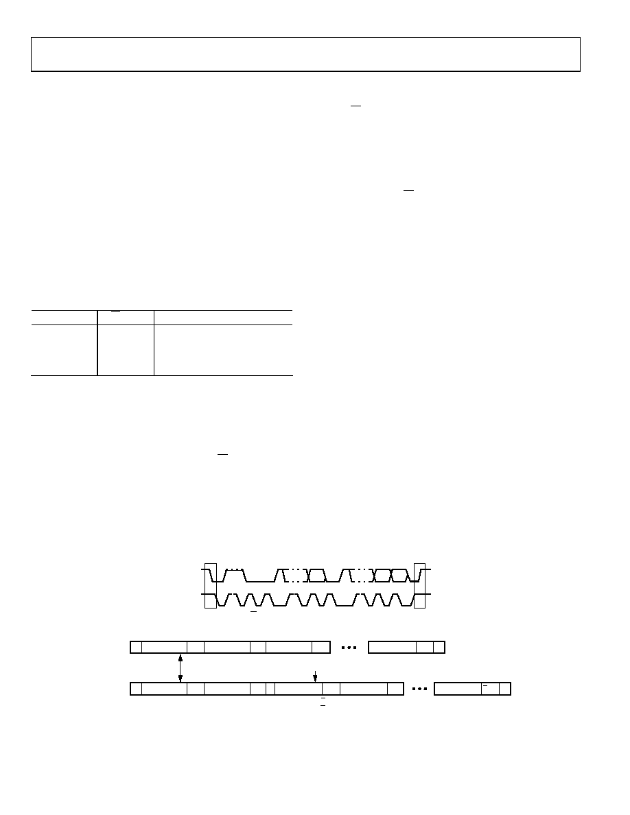
SDATA
SCLOCK
START ADDR
ACK
DATA
ACK
STOP
SUBADDRESS
1–7
8
9
8
9
1–7
8
9
S
P
R/W
Figure 46. Bus Data Transfer
054
79-
050
S
WRITE
SEQUENCE
SLAVE ADDR A(S)
SUB ADDR
A(S)
DATA
A(S)
DATA
A(S) P
S
READ
SEQUENCE
SLAVE ADDR
A(S)
SUB ADDR
A(S) S
A(S)
DATA
A(M)
DATA
A(M) P
S = START BIT
P = STOP BIT
A(S) = ACKNOWLEDGE BY SLAVE
A(M) = ACKNOWLEDGE BY MASTER
A(S) = NO ACKNOWLEDGE BY SLAVE
A(M) = NO ACKNOWLEDGE BY MASTER
LSB = 1
LSB = 0
Figure 47. Read and Write Sequence
相关PDF资料 |
PDF描述 |
|---|---|
| ADV7188BSTZ | IC DECODER VID MULTIFORM 80LQFP |
| ADV7189BBSTZ | IC VIDEO DECODER SDTV 80-LQFP |
| ADV7194KSTZ | IC ENCODER VIDEO EXT-10 80-LQFP |
| ADV7202KSTZ | IC CODEC VIDEO 10BIT 64LQFP |
| ADV7311KST | IC VID ENC 6-12BIT DAC'S 64LQFP |
相关代理商/技术参数 |
参数描述 |
|---|---|
| ADV7185 | 制造商:AD 制造商全称:Analog Devices 功能描述:Professional NTSC/PAL Video Decoder with 10-Bit CCIR656 Output |
| ADV7185KST | 制造商:AD 制造商全称:Analog Devices 功能描述:Professional NTSC/PAL Video Decoder with 10-Bit CCIR656 Output |
| ADV7186 | 制造商:AD 制造商全称:Analog Devices 功能描述:Video Decoder and Display Processor |
| ADV7186BBCZ | 功能描述:IC VIDEO DECODER 196CSPBGA RoHS:是 类别:集成电路 (IC) >> 线性 - 视频处理 系列:- 产品变化通告:Product Discontinuation 07/Mar/2011 标准包装:3,000 系列:OMNITUNE™ 类型:调谐器 应用:移动电话,手机,视频显示器 安装类型:表面贴装 封装/外壳:65-WFBGA 供应商设备封装:PG-WFSGA-65 包装:带卷 (TR) 其它名称:SP000365064 |
| ADV7186BBCZ-RL | 功能描述:IC VIDEO DECODER 196CSPBGA RoHS:是 类别:集成电路 (IC) >> 线性 - 视频处理 系列:- 产品变化通告:Product Discontinuation 07/Mar/2011 标准包装:3,000 系列:OMNITUNE™ 类型:调谐器 应用:移动电话,手机,视频显示器 安装类型:表面贴装 封装/外壳:65-WFBGA 供应商设备封装:PG-WFSGA-65 包装:带卷 (TR) 其它名称:SP000365064 |
发布紧急采购,3分钟左右您将得到回复。