- 您现在的位置:买卖IC网 > PDF目录98007 > M37902FCCHP 16-BIT, FLASH, 26 MHz, MICROCONTROLLER, PQFP100 PDF资料下载
参数资料
| 型号: | M37902FCCHP |
| 元件分类: | 微控制器/微处理器 |
| 英文描述: | 16-BIT, FLASH, 26 MHz, MICROCONTROLLER, PQFP100 |
| 封装: | 14 X 14 MM, 0.50 MM PITCH, PLASTIC, LQFP-100 |
| 文件页数: | 100/143页 |
| 文件大小: | 1148K |
| 代理商: | M37902FCCHP |
第1页第2页第3页第4页第5页第6页第7页第8页第9页第10页第11页第12页第13页第14页第15页第16页第17页第18页第19页第20页第21页第22页第23页第24页第25页第26页第27页第28页第29页第30页第31页第32页第33页第34页第35页第36页第37页第38页第39页第40页第41页第42页第43页第44页第45页第46页第47页第48页第49页第50页第51页第52页第53页第54页第55页第56页第57页第58页第59页第60页第61页第62页第63页第64页第65页第66页第67页第68页第69页第70页第71页第72页第73页第74页第75页第76页第77页第78页第79页第80页第81页第82页第83页第84页第85页第86页第87页第88页第89页第90页第91页第92页第93页第94页第95页第96页第97页第98页第99页当前第100页第101页第102页第103页第104页第105页第106页第107页第108页第109页第110页第111页第112页第113页第114页第115页第116页第117页第118页第119页第120页第121页第122页第123页第124页第125页第126页第127页第128页第129页第130页第131页第132页第133页第134页第135页第136页第137页第138页第139页第140页第141页第142页第143页
M37902FCCHP, M37902FGCHP, M37902FJCHP
SINGLE-CHIP 16-BIT CMOS MICROCOMPUTER
MITSUBISHI MICROCOMPUTERS
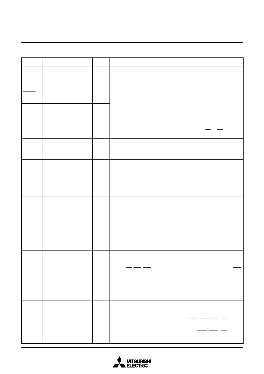
6
Vcc, Vss
MD0
MD1
RESET
XIN
XOUT
BYTE
VCONT
AVcc,
AVss
VREF
P00–P07
P10–P17
P20–P27
P30–P33
P40–P47
Power supply input
MD0
MD1
Reset input
Clock input
Clock output
External data bus width
select input
Filter circuit connection
Analog power supply input
Reference voltage input
I/O port P0
I/O port P1
I/O port P2
I/O port P3
I/O port P4
—
Input
Output
Input
—
Input
I/O
Apply 5 V±0.5 V to Vcc, and 0 V to Vss.
This pin controls the processor mode. Connect this pin to VSS for the single-chip
mode or memory expansion mode, and VCC for the microprocessor mode.
Connect this pin to Vss.
The microcomputer is reset when “L” level is applied to this pin.
These are input and output pins of the internal clock generating circuit. Connect a
ceramic or quartz- crystal resonator between the XIN and XOUT pins. When an
external clock is used, the clock source should be connected to the XIN pin, and the
XOUT pin should be left open.
This pin determines whether the external data bus has an 8-bit width or 16-bit width
for the memory expansion mode or microprocessor mode. The width is 16 bits when
“L” signal is input, and 8 bits when “H” signal is input. When BYTE = Vss level, by
the register setting, the external data bus for each of areas CS1 to CS3 can have a
width of 8 bits.
When using the PLL frequency multiplier, connect this pin to the filter circuit. When
not using, this pin should be left open.
Power supply input pins for the A-D converter and the D-A converter. Connect AVcc
to Vcc, and AVss to Vss externally.
This is the reference voltage input pin for the A-D converter and the D-A converter.
s In single-chip mode
Port P0 is an 8-bit I/O port. This port has an I/O direction register, and each pin
can be programmed for input or output. These pins enter the input mode at
reset.
s In memory expansion and microprocessor modes
Address (A16–A23) is output. These pins also function as I/O port pins according
to the register setting.
s In single-chip mode
These pins have the same functions as port P0.
s In memory expansion and microprocessor modes
The low-order 8 bits of data (D0–D7) are input/output. When the external data bus
has an 8-bit width, address (LA0–LA7) output and data (D0–D7) input/output can
be performed with the time-sharing method, according to the register setting.
s In single-chip mode or When 8-bit external data bus is used in memory expansion
mode and microprocessor mode
These pins have the same functions as port P0.
s When the 16-bit external data bus is used in memory expansion or microproce-
ssor mode
The high-order 8 bits of data (D8–D15) are input or output.
s In single-chip mode
These pins have the same functions as port P0.
s In memory expansion mode
P30 functions as an I/O port pin; and P31, P32, and P33 function as the output
pins of RD, BLW, BHW, respectively. P30 also functions as an output pin of RDY
according to the register setting. When the external data bus has a width of 8 bits,
the BHW pin functions as an I/O port pin (P33).
s In microprocessor mode
P30 functions as an input pin of RDY; and P31,P32, P33 function as the output
pins of RD, BLW, BHW, respectively. P30 also functions as an I/O port pin accord-
ing to the register setting. When the external data bus has a width of 8 bits,
the BHW pin functions as an I/O port pin (P33).
s In single-chip mode
These pins have the same functions as port P0.
s In memory expansion mode
P40–P47 function as I/O port pins. According to the register setting, these pins
function as output pins or input pins of ALE,
φ1, HLDA, HOLD, CS0–CS3, respec-
tively.
s In microprocessor mode
P40–P44 function as output or input pins of ALE,
φ1, HLDA, HOLD, CS0, and
P45–P47 as I/O port pins, respectively. According to the register setting, P40–P43
also function as I/O port pins, and P45–P47 as output pins of CS1–CS3.
PIN DESCRIPTION (MICROCOMPUTER MODE)
Functions
Input/
Output
Name
Pin
相关PDF资料 |
PDF描述 |
|---|---|
| M37902FGCHP | 16-BIT, FLASH, 26 MHz, MICROCONTROLLER, PQFP100 |
| M37906F8CSP | 16-BIT, FLASH, 20 MHz, MICROCONTROLLER, PDIP42 |
| M37906F8CFP | 16-BIT, FLASH, 20 MHz, MICROCONTROLLER, PDSO42 |
| M37906F8CSP | 16-BIT, FLASH, 20 MHz, MICROCONTROLLER, PDIP42 |
| M37920S4CGP | 16-BIT, 20 MHz, MICROCONTROLLER, PQFP100 |
相关代理商/技术参数 |
参数描述 |
|---|---|
| M37902FGCGP | 制造商:MITSUBISHI 制造商全称:Mitsubishi Electric Semiconductor 功能描述:SINGLE-CHIP 16-BIT CMOS MICROCOMPUTER |
| M37902FGCHP | 制造商:MITSUBISHI 制造商全称:Mitsubishi Electric Semiconductor 功能描述:SINGLE-CHIP 16-BIT CMOS MICROCOMPUTER |
| M37902FJCHP | 制造商:MITSUBISHI 制造商全称:Mitsubishi Electric Semiconductor 功能描述:SINGLE-CHIP 16-BIT CMOS MICROCOMPUTER |
| M37903S4CHP | 制造商:RENESAS 制造商全称:Renesas Technology Corp 功能描述:16-BIT CMOS MICROCOMPUTER |
| M37905F8CFP | 制造商:MITSUBISHI 制造商全称:Mitsubishi Electric Semiconductor 功能描述:16-BIT CMOS MICROCOMPUTER |
发布紧急采购,3分钟左右您将得到回复。