- 您现在的位置:买卖IC网 > PDF目录98007 > M37902FCCHP 16-BIT, FLASH, 26 MHz, MICROCONTROLLER, PQFP100 PDF资料下载
参数资料
| 型号: | M37902FCCHP |
| 元件分类: | 微控制器/微处理器 |
| 英文描述: | 16-BIT, FLASH, 26 MHz, MICROCONTROLLER, PQFP100 |
| 封装: | 14 X 14 MM, 0.50 MM PITCH, PLASTIC, LQFP-100 |
| 文件页数: | 103/143页 |
| 文件大小: | 1148K |
| 代理商: | M37902FCCHP |
第1页第2页第3页第4页第5页第6页第7页第8页第9页第10页第11页第12页第13页第14页第15页第16页第17页第18页第19页第20页第21页第22页第23页第24页第25页第26页第27页第28页第29页第30页第31页第32页第33页第34页第35页第36页第37页第38页第39页第40页第41页第42页第43页第44页第45页第46页第47页第48页第49页第50页第51页第52页第53页第54页第55页第56页第57页第58页第59页第60页第61页第62页第63页第64页第65页第66页第67页第68页第69页第70页第71页第72页第73页第74页第75页第76页第77页第78页第79页第80页第81页第82页第83页第84页第85页第86页第87页第88页第89页第90页第91页第92页第93页第94页第95页第96页第97页第98页第99页第100页第101页第102页当前第103页第104页第105页第106页第107页第108页第109页第110页第111页第112页第113页第114页第115页第116页第117页第118页第119页第120页第121页第122页第123页第124页第125页第126页第127页第128页第129页第130页第131页第132页第133页第134页第135页第136页第137页第138页第139页第140页第141页第142页第143页
62
M37902FCCHP, M37902FGCHP, M37902FJCHP
SINGLE-CHIP 16-BIT CMOS MICROCOMPUTER
MITSUBISHI MICROCOMPUTERS
(2) Event counter mode [01]
Figure 60 shows the bit configuration of the timer Bi mode register
during event counter mode. In event counter mode, bit 0 in the timer
Bi mode register must be “1” and bit 1 must be “0”.
The input signal from the TBiIN pin is counted when the count start
bit is “1” and counting is stopped when it is “0”.
Count is performed at the fall of the input signal when bits 2, and 3
are “0” and at the rise of the input signal when bit 3 is “0” and bit 2 is
“1”.
When bit 3 is “1” and bit 2 is “0”, count is performed at the rise and
fall of the input signal.
Data write, data read and timer interrupt are performed in the same
way as for timer mode.
Only for timer B2, when the timer B2 clock source select bit of the
particular function select register 1 (bit 6 at address 6316) = “1” in the
event counter mode, fX32 can be selected. (When this bit is “0”, an
input signal from pin TB2IN becomes the count source as described
above.) For the bit configuration of the particular function select reg-
ister 1, refer to the section on the standby function.
Note: fX32 = f(XIN)/32
(3) Pulse period measurement/Pulse width
measurement mode [10]
Figure 61 shows the bit configuration of the timer Bi mode register
during pulse period measurement/pulse width measurement mode.
In pulse period measurement/pulse width measurement mode, bit 0
must be “0” and bit 1 must be “1”. Bits 6 and 7 are used to select the
clock source. The selected clock is counted when the count start bit
is “1” and counting stops when it is “0”.
The pulse period measurement mode is selected when bit 3 is “0”. In
pulse period measurement mode, the selected clock is counted dur-
ing the interval starting at the fall of the input signal from the TBiIN pin
to the next fall or at the rise of the input signal to the next rise; the
result is stored in the reload register. In this case, the reload register
acts as a buffer register.
When bit 2 is “0”, the clock is counted from the fall of the input signal
to the next fall. When bit 2 is “1“, the clock is counted from the rise of
the input signal to the next rise.
In the case of counting from the fall of the input signal to the next fall,
counting is performed as follows. As shown in Figure 62, when the
fall of the input signal from TBiIN pin is detected, the contents of the
counter is transferred to the reload register. Next, the counter is
cleared and count is started from the next clock. When the fall of the
next input signal is detected, the contents of the counter is trans-
ferred to the reload register once more, the counter is cleared, and
the count is started. The period from the fall of the input signal to the
next fall is measured in this way.
After the contents of the counter is transferred to the reload register,
an interrupt request signal is generated and the interrupt request bit
in the timer Bi interrupt control register is set. However, no interrupt
request signal is generated when the contents of the counter is trans-
ferred first to the reload register after the count start bit is set to “1”.
When bit 3 is “1”, the pulse width measurement mode is selected.
Pulse width measurement mode is the same as the pulse period
measurement mode except that the clock is counted from the fall of
the TBiIN pin input signal to the next rise or from the rise of the input
signal to the next fall as shown in Figure 63.
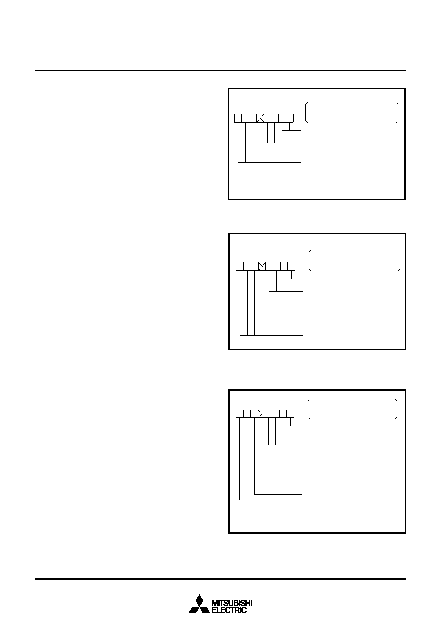
Fig. 59 Bit configuration of timer Bi mode register during timer mode
Fig. 60 Bit configuration of timer Bi mode register during event
counter mode
Fig. 61 Bit configuration of timer Bi mode register during pulse period
measurement/pulse width measurement mode
0 0 : Always “00” in timer mode
× × : Not used in timer mode and
may be any
Not used in timer mode
Clock source select bits
0 0 : Select f2
0 1 : Select f16
1 0 : Select f64
1 1 : Select f512
76543210
0
×
Timer B0 mode register
Timer B1 mode register
Timer B2 mode register
Addresses
5B16
5C16
5D16
0 1 : Always “01” in event counter
mode
0 0 : Count at the falling edge of
input signal
0 1 : Count at the rising edge of
input signal
1 0 : Count at the both falling edge
and rising edge of input signal
× × × : Not used in event counter mode
76543210
1
0
×
Timer B0 mode register
Timer B1 mode register
Timer B2 mode register
Addresses
5B16
5C16
5D16
1 0 : Always “10” in pulse period
measurement/pulse width
measurement mode
0 0 : Count from the falling edge of
input signal to the next falling one
0 1 : Count from the rising edge of
input signal to the next rising one
1 0 : Count from the falling edge of
input signal to the next rising one
and from the rising edge to the
next falling one
Timer Bi overflow flag
Clock source select bits
0 0 : Select f2
0 1 : Select f16
1 0 : Select f64
1 1 : Select f512
76543210
0
1
Timer B0 mode register
Timer B1 mode register
Timer B2 mode register
Addresses
5B16
5C16
5D16
相关PDF资料 |
PDF描述 |
|---|---|
| M37902FGCHP | 16-BIT, FLASH, 26 MHz, MICROCONTROLLER, PQFP100 |
| M37906F8CSP | 16-BIT, FLASH, 20 MHz, MICROCONTROLLER, PDIP42 |
| M37906F8CFP | 16-BIT, FLASH, 20 MHz, MICROCONTROLLER, PDSO42 |
| M37906F8CSP | 16-BIT, FLASH, 20 MHz, MICROCONTROLLER, PDIP42 |
| M37920S4CGP | 16-BIT, 20 MHz, MICROCONTROLLER, PQFP100 |
相关代理商/技术参数 |
参数描述 |
|---|---|
| M37902FGCGP | 制造商:MITSUBISHI 制造商全称:Mitsubishi Electric Semiconductor 功能描述:SINGLE-CHIP 16-BIT CMOS MICROCOMPUTER |
| M37902FGCHP | 制造商:MITSUBISHI 制造商全称:Mitsubishi Electric Semiconductor 功能描述:SINGLE-CHIP 16-BIT CMOS MICROCOMPUTER |
| M37902FJCHP | 制造商:MITSUBISHI 制造商全称:Mitsubishi Electric Semiconductor 功能描述:SINGLE-CHIP 16-BIT CMOS MICROCOMPUTER |
| M37903S4CHP | 制造商:RENESAS 制造商全称:Renesas Technology Corp 功能描述:16-BIT CMOS MICROCOMPUTER |
| M37905F8CFP | 制造商:MITSUBISHI 制造商全称:Mitsubishi Electric Semiconductor 功能描述:16-BIT CMOS MICROCOMPUTER |
发布紧急采购,3分钟左右您将得到回复。