- 您现在的位置:买卖IC网 > PDF目录299768 > PF38F3352LLZDQ0 (INTEL CORP) SPECIALTY MEMORY CIRCUIT, PBGA88 PDF资料下载
参数资料
| 型号: | PF38F3352LLZDQ0 |
| 厂商: | INTEL CORP |
| 元件分类: | 存储器 |
| 英文描述: | SPECIALTY MEMORY CIRCUIT, PBGA88 |
| 封装: | 11 X 13 MM, SCSP-88 |
| 文件页数: | 16/54页 |
| 文件大小: | 966K |
| 代理商: | PF38F3352LLZDQ0 |
第1页第2页第3页第4页第5页第6页第7页第8页第9页第10页第11页第12页第13页第14页第15页当前第16页第17页第18页第19页第20页第21页第22页第23页第24页第25页第26页第27页第28页第29页第30页第31页第32页第33页第34页第35页第36页第37页第38页第39页第40页第41页第42页第43页第44页第45页第46页第47页第48页第49页第50页第51页第52页第53页第54页
768-Mbit LVQ Family with Asynchronous Static RAM
Datasheet
23
6.0
Electrical Specifications
6.1
DC Current Characteristics
The DC current characteristics referenced in this document are for individual flash and RAM die in
the SCSP device. The total device current is determined by sum of the active and inactive currents
of each flash and RAM die in the SCSP device.
Note:
Refer to the latest revision of the Intel StrataFlash
Wireless Memory System (LV18/LV30 SCSP;
1024-Mbit LV Family Datasheet (order number 253854) for flash DC characteristics not included
in this document.
NOTICE: Individual DC Characteristics of all dies in a SCSP device need to be considered
accordingly, depending on the SCSP device stacked combinations and operations.
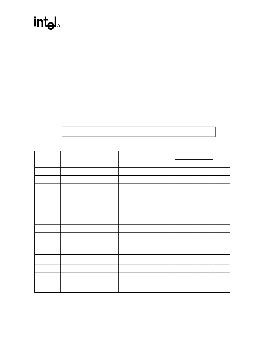
Table 5.
SRAM DC Characteristics
Parameter
Description
Test Conditions
3.0 V SRAM
Unit
MIN
MAX
S-VCC
Voltage Range
–
2.7
3.3
V
VDR
S-VCC for Data Retention
–
1.5
–
V
ICC
Operating Current at minimum cycle
time
IIO =0 mA
–
50
mA
ICC2
Operating Current at maximum
cycle time (1
s)
IIO =0 mA
–
10
mA
ISB
Standby Current
S-CS1#
≥ S-V
CC-0.2V
or S-CS2
≤ V
SS+0.2V
Address/Data toggling at minimum
cycle time
–25
A
IDR
Current in Data Retention mode
S-VCC =1.5 V
–
12
A
VOH
Output High Voltage
IOH =-100 A
S-VCC -
0.1
–V
VOL
Output Low Voltage
IOL =100 A,
VCCMIN
-0.1
0.1
V
VIH
Input High Voltage
–
S-VCC -
0.4
S-VCC+
0.2
V
VIL
Input Low Voltage
–
-0.2
0.6
V
*IIL
Input Leakage Current
-0.2 < VIN <S-VCC+0.2 V
-1
+1
A
*ILDR
Input Leakage Current in Data
Retention Mode
-0.2 < VIN <S-VCC+0.2 V
S-VCC =VDR
-1
+1
A
NOTE:
* Input leakage currents include Hi-Z output leakage for bi-directional buffers with tri-state outputs.
相关PDF资料 |
PDF描述 |
|---|---|
| PF38F40L0YUQ0 | 16M X 16 FLASH 1.8V PROM, PBGA88 |
| PF50WIW2K-3.5VF-W6 | SINGLE COLOR LED, INCAND WHITE |
| PD50WO3K-28V-T | SINGLE COLOR LED, SUPER ORANGE |
| PD50WR3K-24V-W6 | SINGLE COLOR LED, ULTRA RED |
| PF50WAG6K-240VAC-W6 | SINGLE COLOR LED, AQUA GREEN |
相关代理商/技术参数 |
参数描述 |
|---|---|
| PF38F4040L0YWA | 制造商:Micron Technology Inc 功能描述:256LCR/32PS SCSP 1.8 HF NOKIA - Tape and Reel |
| PF38F4040L0YWAGB | 制造商:Micron Technology Inc 功能描述:WIRELESS - Tape and Reel |
| PF38F4050L0YWQEA | 制造商:Micron Technology Inc 功能描述:WIRELESS - Trays |
| PF38F4050L0ZTQ0 | 制造商:Intel 功能描述:MM#869453 FLASH |
| PF38F4050M0Y0CEA | 制造商:Micron Technology Inc 功能描述:WIRELESS - Trays |
发布紧急采购,3分钟左右您将得到回复。