- 您现在的位置:买卖IC网 > PDF目录299768 > PF38F3352LLZDQ0 (INTEL CORP) SPECIALTY MEMORY CIRCUIT, PBGA88 PDF资料下载
参数资料
| 型号: | PF38F3352LLZDQ0 |
| 厂商: | INTEL CORP |
| 元件分类: | 存储器 |
| 英文描述: | SPECIALTY MEMORY CIRCUIT, PBGA88 |
| 封装: | 11 X 13 MM, SCSP-88 |
| 文件页数: | 29/54页 |
| 文件大小: | 966K |
| 代理商: | PF38F3352LLZDQ0 |
第1页第2页第3页第4页第5页第6页第7页第8页第9页第10页第11页第12页第13页第14页第15页第16页第17页第18页第19页第20页第21页第22页第23页第24页第25页第26页第27页第28页当前第29页第30页第31页第32页第33页第34页第35页第36页第37页第38页第39页第40页第41页第42页第43页第44页第45页第46页第47页第48页第49页第50页第51页第52页第53页第54页
768-Mbit LVQ Family with Asynchronous Static RAM
Datasheet
35
9.0
Design Guide: Operation Overview
9.1
Bus Operations
With F-CE# low and F-RST# high, the flash dies are enabled for normal operations. The flash
device internally decodes upper address inputs to determine the accessed partition or block.
In an asynchronous read operation, addresses are latched when ADV# transition from VIL to VIH,
or continuously flows through if ADV# is held low. In synchronous-burst mode, addresses are
latched by the rising edge of ADV# or the next valid CLK edge when ADV# is low.
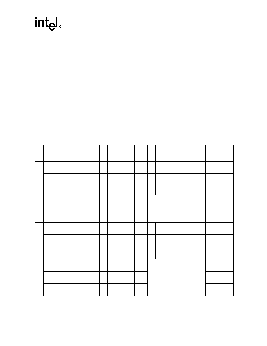
Table 13, “Flash + PSRAM + SRAM Bus Operations” summarizes the bus operations and voltage
levels that must be applied to individual flash die in each mode
Note:
Each flash die within the 768-Mbit LVQ Family with Asynchronous Static RAM device shares
basic asynchronous read and write operations unless otherwise specified.
Table 13. Flash + PSRAM + SRAM Bus Operations (Sheet 1 of 2)
D
evi
ce
Mo
d
e
F-
R
S
T#
F1
-C
E
#
F2
-C
E
#
F-
O
E
#
F-
WE
#
WA
IT
AD
V#
F-
V
P
S-
C
S
1
#
S-
C
S
2
P-
M
o
de
P-
C
S
#
R-
OE#
R-
W
E
#
R-
UB#
,
R-
L
B
#
D[
1
5
:0
]
No
te
s
Fl
as
hD
ie
#1
(c
o
d
e
)
Synchronous
Array and Non-
Array Read
HL
H
Active
L
X
H
X
H
XX
X
Flash
DOUT
1,2,3,4
,5,6,9
Asynchronous
Read
H
L
H
L
H
Deasserted
L
X
H
XX
H
XX
X
Flash
DOUT
1,2,3,4
,5,6,9
Write
H
L
H
L
Deasserted
L
VPP1
or
VPP2
H
XX
H
XX
X
Flash
DIN
3,4,6
Output Disable
H
L
H
High-Z
X
High-Z
Any xSRAM mode allowed
Flash
High-Z
4
Standby
H
X
High-Z
X
High-Z
Flash
High-Z
4
Reset
L
XXXX
High-Z
X
High-Z
Flash
High-Z
4
Fl
as
h
D
ie
#
2
(d
at
a
)
Synchronous
Array and Non-
Array Read
H
L
H
Deasserted
L
X
HX
X
H
X
Flash
Die #2
DOUT
1,2,3,4
,5,6,9
Async Read
H
L
H
Deasserted
L
X
HX
X
H
X
Flash
Die #2
DOUT
1,2,3,4
,5,6,9
Write
H
L
H
L
Deasserted
L
Vpp1
or
Vpp2
HX
X
H
X
Flash
Die #2
DOUT
3,4,6
Output Disable
H
L
H
High-Z
X
High-Z
Any xSRAM mode allowed
Flash#
2 High-
Z
4
Standby
H
X
High-Z
X
High-Z
Flash
#2
High-Z
4
Reset
L
XXXX
High-Z
X
High-Z
Flash
#2
High-Z
4
相关PDF资料 |
PDF描述 |
|---|---|
| PF38F40L0YUQ0 | 16M X 16 FLASH 1.8V PROM, PBGA88 |
| PF50WIW2K-3.5VF-W6 | SINGLE COLOR LED, INCAND WHITE |
| PD50WO3K-28V-T | SINGLE COLOR LED, SUPER ORANGE |
| PD50WR3K-24V-W6 | SINGLE COLOR LED, ULTRA RED |
| PF50WAG6K-240VAC-W6 | SINGLE COLOR LED, AQUA GREEN |
相关代理商/技术参数 |
参数描述 |
|---|---|
| PF38F4040L0YWA | 制造商:Micron Technology Inc 功能描述:256LCR/32PS SCSP 1.8 HF NOKIA - Tape and Reel |
| PF38F4040L0YWAGB | 制造商:Micron Technology Inc 功能描述:WIRELESS - Tape and Reel |
| PF38F4050L0YWQEA | 制造商:Micron Technology Inc 功能描述:WIRELESS - Trays |
| PF38F4050L0ZTQ0 | 制造商:Intel 功能描述:MM#869453 FLASH |
| PF38F4050M0Y0CEA | 制造商:Micron Technology Inc 功能描述:WIRELESS - Trays |
发布紧急采购,3分钟左右您将得到回复。