- 您现在的位置:买卖IC网 > Datasheet目录354 > RC28F00BM29EWHA (Micron Technology Inc)IC FLASH 2GBIT 100NS 64FBGA Datasheet资料下载
参数资料
| 型号: | RC28F00BM29EWHA |
| 厂商: | Micron Technology Inc |
| 文件页数: | 25/75页 |
| 文件大小: | 0K |
| 描述: | IC FLASH 2GBIT 100NS 64FBGA |
| 标准包装: | 184 |
| 系列: | Axcell™ |
| 格式 - 存储器: | 闪存 |
| 存储器类型: | 闪存 - 或非 |
| 存储容量: | 2G(256M x 8,128M x 16) |
| 速度: | 100ns |
| 接口: | 并联 |
| 电源电压: | 2.7 V ~ 3.6 V |
| 工作温度: | -40°C ~ 85°C |
| 封装/外壳: | 64-LBGA |
| 供应商设备封装: | 64-FBGA(11x13) |
| 包装: | 托盘 |
第1页第2页第3页第4页第5页第6页第7页第8页第9页第10页第11页第12页第13页第14页第15页第16页第17页第18页第19页第20页第21页第22页第23页第24页当前第25页第26页第27页第28页第29页第30页第31页第32页第33页第34页第35页第36页第37页第38页第39页第40页第41页第42页第43页第44页第45页第46页第47页第48页第49页第50页第51页第52页第53页第54页第55页第56页第57页第58页第59页第60页第61页第62页第63页第64页第65页第66页第67页第68页第69页第70页第71页第72页第73页第74页第75页
�� �
�
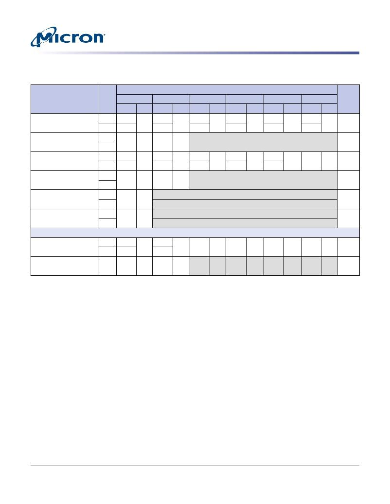
�256Mb,� 512Mb,� 1Gb,� 2Gb:� 3V� Embedded� Parallel� NOR� Flash�
�Standard� Command� Definitions� –� Address-Data� Cycles�
�Table� 11:� Standard� Command� Definitions� –� Address-Data� Cycles,� 8-Bit� and� 16-Bit� (Continued)�
�Note� 1� applies� to� entire� table�
�Address and� Data� Cycles�
�Command� and�
�Bus�
�1st�
�2nd�
�3rd�
�4th�
�5th�
�6th�
�Code/Subcode�
�CHIP� ERASE� (80/10h)�
�Size�
�x8�
�A�
�AAA�
�D�
�AA�
�A�
�555�
�D�
�55�
�A�
�AAA�
�D�
�80�
�A�
�AAA�
�D�
�AA�
�A�
�555�
�D�
�55�
�A�
�AAA�
�D�
�10�
�Notes�
�x16�
�555�
�2AA�
�555�
�555�
�2AA�
�555�
�UNLOCK� BYPASS�
�x8�
�X�
�80�
�X�
�10�
�5�
�CHIP� ERASE� (80/10h)�
�x16�
�BLOCK� ERASE� (80/30h)�
�x8�
�AAA�
�AA�
�555�
�55�
�AAA�
�80�
�AAA�
�AA�
�555�
�55�
�BAd�
�30�
�9�
�x16�
�555�
�2AA�
�555�
�555�
�2AA�
�UNLOCK� BYPASS�
�x8�
�X�
�80�
�BAd�
�30�
�5�
�BLOCK� ERASE� (80/30h)�
�x16�
�ERASE� SUSPEND� (B0h)�
�x8�
�X�
�B0�
�x16�
�ERASE� RESUME� (30h)�
�x8�
�X�
�30�
�x16�
�BLANK� CHECK� Operations�
�BLANK� CHECK�
�x8�
�AAA�
�AA�
�555�
�55�
�BAd�
�EB�
�BAd�
�76�
�BAd�
�00�
�BAd�
�00�
�SETUP� (EB/76h)�
�x16�
�555�
�2AA�
�BLANK� CHECK� CONFIRM�
�x8�
�BAd�
�29�
�BAd�
�Note�
�2�
�and� READ� (29h)�
�x16�
�Notes:�
�2�
�1.� A� =� Address;� D� =� Data;� X� =� "Don't� Care;"� BAd� =� Any� address� in� the� block;� N� =� Number� of�
�bytes� to� be� programmed;� PA� =� Program� address;� PD� =� Program� data;� Gray� shading� =� Not�
�applicable.� All� values� in� the� table� are� hexadecimal.� Some� commands� require� both� a� com-�
�mand� code� and� subcode.� For� the� 2Gb� device,� the� set-up� command� must� be� issued� for�
�each� selected� die.�
�2.� These� cells� represent� READ� cycles� (versus� WRITE� cycles� for� the� others).�
�3.� AUTO� SELECT� enables� the� device� to� read� the� manufacturer� code,� device� code,� block� pro-�
�tection� status,� and� extended� memory� block� protection� indicator.�
�4.� AUTO� SELECT� addresses� and� data� are� specified� in� the� Electronic� Signature� table� and� the�
�Extended� Memory� Block� Protection� table.�
�5.� For� any� UNLOCK� BYPASS� ERASE/PROGRAM� command,� the� first� two� UNLOCK� cycles� are�
�unnecessary.�
�6.� BAd� must� be� the� same� as� the� address� loaded� during� the� WRITE� TO� BUFFER� PROGRAM�
�3rd� and� 4th� cycles.�
�7.� WRITE� TO� BUFFER� PROGRAM� operation:� maximum� cycles� =� 261� (x8)� and� 517� (x16).� UN-�
�LOCK� BYPASS� WRITE� TO� BUFFER� PROGRAM� operation:� maximum� cycles� =� 259� (x8),� 515�
�(x16).� WRITE� TO� BUFFER� PROGRAM� operation:� N� +� 1� =� bytes� to� be� programmed;� maxi-�
�mum� buffer� size� =� 256� bytes� (x8)� and� 1024� bytes� (x16).�
�8.� For� x8,� A[MAX:7]� address� pins� should� remain� unchanged� while� A[6:0]� and� A-1� pins� are�
�used� to� select� a� byte� within� the� N� +� 1� byte� page.� For� x16,� A[MAX:9]� address� pins� should�
�remain� unchanged� while� A[8:0]� pins� are� used� to� select� a� word� within� the� N+1� word�
�page.�
�9.� BLOCK� ERASE� address� cycles� can� extend� beyond� six� address-data� cycles,� depending� on�
�the� number� of� blocks� to� erase.�
�PDF:� 09005aef849b4b09�
�m29ew_256mb_2gb.pdf� -� Rev.� B� 8/12� EN�
�25�
�Micron� Technology,� Inc.� reserves� the� right� to� change� products� or� specifications� without� notice.�
�?� 2012� Micron� Technology,� Inc.� All� rights� reserved.�
�相关PDF资料 |
PDF描述 |
|---|---|
| RDK-242 | KIT REF DESIGN VG TOPSWITCH-JX |
| RJCSE538001 | CONN MOD JACK 8P8C SMT R/A |
| RJE031882420 | CONN MOD JACK 8P/8C S-FLANGES |
| RJE051660310 | CONN MOD JACK 6P/6C UNSHIELDED |
| RJE051880110 | CONN MOD JACK 8/8 R/A UNSHIELDED |
相关代理商/技术参数 |
参数描述 |
|---|---|
| RC28F128J3A_13 | 制造商:INTEL 制造商全称:Intel Corporation 功能描述:Intel StrataFlash?? Memory |
| RC28F128J3A-110 | 制造商:INTEL 制造商全称:Intel Corporation 功能描述:Intel StrataFlash Memory (J3) |
| RC28F128J3A-115 | 制造商:INTEL 制造商全称:Intel Corporation 功能描述:Intel StrataFlash Memory (J3) |
| RC28F128J3A-120 | 制造商:INTEL 制造商全称:Intel Corporation 功能描述:Intel StrataFlash Memory (J3) |
| RC28F128J3A-125 | 制造商:INTEL 制造商全称:Intel Corporation 功能描述:Intel StrataFlash Memory (J3) |
发布紧急采购,3分钟左右您将得到回复。