- 您现在的位置:买卖IC网 > Datasheet目录354 > RC28F00BM29EWHA (Micron Technology Inc)IC FLASH 2GBIT 100NS 64FBGA Datasheet资料下载
参数资料
| 型号: | RC28F00BM29EWHA |
| 厂商: | Micron Technology Inc |
| 文件页数: | 30/75页 |
| 文件大小: | 0K |
| 描述: | IC FLASH 2GBIT 100NS 64FBGA |
| 标准包装: | 184 |
| 系列: | Axcell™ |
| 格式 - 存储器: | 闪存 |
| 存储器类型: | 闪存 - 或非 |
| 存储容量: | 2G(256M x 8,128M x 16) |
| 速度: | 100ns |
| 接口: | 并联 |
| 电源电压: | 2.7 V ~ 3.6 V |
| 工作温度: | -40°C ~ 85°C |
| 封装/外壳: | 64-LBGA |
| 供应商设备封装: | 64-FBGA(11x13) |
| 包装: | 托盘 |
第1页第2页第3页第4页第5页第6页第7页第8页第9页第10页第11页第12页第13页第14页第15页第16页第17页第18页第19页第20页第21页第22页第23页第24页第25页第26页第27页第28页第29页当前第30页第31页第32页第33页第34页第35页第36页第37页第38页第39页第40页第41页第42页第43页第44页第45页第46页第47页第48页第49页第50页第51页第52页第53页第54页第55页第56页第57页第58页第59页第60页第61页第62页第63页第64页第65页第66页第67页第68页第69页第70页第71页第72页第73页第74页第75页
�� �
�
�256Mb,� 512Mb,� 1Gb,� 2Gb:� 3V� Embedded� Parallel� NOR� Flash�
�Program� Operations�
�First,� two� UNLOCK� cycles� are� issued.� Next,� a� third� bus� WRITE� cycle� sets� up� the� WRITE�
�TO� BUFFER� PROGRAM� command.� The� set-up� code� can� be� addressed� to� any� location�
�within� the� targeted� block.� Then,� a� fourth� bus� WRITE� cycle� sets� up� the� number� of� words/�
�bytes� to� be� programmed.� Value� n� is� written� to� the� same� block� address,� where� n� +� 1� is� the�
�number� of� words/bytes� to� be� programmed.� Value� n� +� 1� must� not� exceed� the� size� of� the�
�program� buffer,� or� the� operation� will� abort.� A� fifth� cycle� loads� the� first� address� and� data�
�to� be� programmed.� Last,� n� bus� WRITE� cycles� load� the� address� and� data� for� each� word/�
�byte� into� the� program� buffer.� Addresses� must� lie� within� the� range� from� the� start� address�
�+1� to� the� start� address� +� (n� -� 1)� .�
�Optimum� programming� performance� and� lower� power� usage� are� achieved� by� aligning�
�the� starting� address� at� the� beginning� of� a� 512-word� boundary� (A[8:0]� =� 0x000h).� Any�
�buffer� size� smaller� than� 512� words� is� allowed� within� a� 512-word� boundary,� while� all� ad-�
�dresses� used� in� the� operation� must� lie� within� the� 512-word� boundary.� In� addition,� any�
�crossing� boundary� buffer� program� will� result� in� a� program� abort.� For� a� x8� device,� maxi-�
�mum� buffer� size� is� 256� bytes;� for� a� x16� device,� the� maximum� buffer� size� is� 1024� bytes.�
�To� program� the� content� of� the� program� buffer,� this� command� must� be� followed� by� a�
�WRITE� TO� BUFFER� PROGRAM� CONFIRM� command.�
�If� an� address� is� written� several� times� during� a� WRITE� TO� BUFFER� PROGRAM� operation,�
�the� address/data� counter� will� be� decremented� at� each� data� load� operation,� and� the� data�
�will� be� programmed� to� the� last� word� loaded� into� the� buffer.�
�Invalid� address� combinations� or� the� incorrect� sequence� of� bus� WRITE� cycles� will� abort�
�the� WRITE� TO� BUFFER� PROGRAM� command.�
�The� status� register� bits� DQ1,� DQ5,� DQ6,� DQ7� can� be� used� to� monitor� the� device� status�
�during� a� WRITE� TO� BUFFER� PROGRAM� operation.�
�The� WRITE� TO� BUFFER� PROGRAM� command� should� not� be� used� to� change� a� bit� set� to�
�0� back� to� 1,� and� an� attempt� to� do� so� is� masked� during� the� operation.� Rather� than� the�
�WRITE� TO� BUFFER� PROGRAM� command,� the� ERASE� command� should� be� used� to� set�
�memory� bits� from� 0� to� 1.�
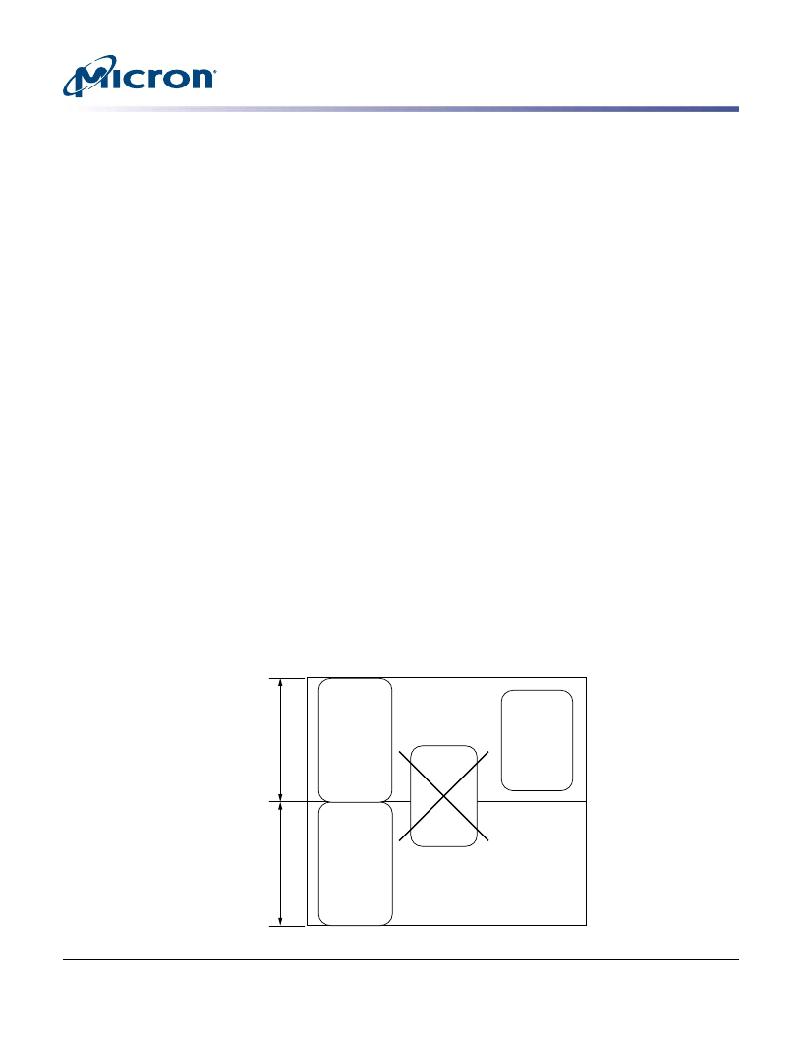
�Figure� 9:� Boundary� Condition� of� Program� Buffer� Size�
�0000h�
�512� Words�
�0200h�
�512-word�
�program�
�buffer� is�
�allowed�
�Any�
�buffer�
�program�
�attempt�
�511� words�
�or� less� are�
�allowed�
�in� the�
�program�
�buffer�
�is� not�
�512� Words�
�512-word�
�program�
�allowed�
�buffer� is�
�allowed�
�0400h�
�PDF:� 09005aef849b4b09�
�m29ew_256mb_2gb.pdf� -� Rev.� B� 8/12� EN�
�30�
�Micron� Technology,� Inc.� reserves� the� right� to� change� products� or� specifications� without� notice.�
�?� 2012� Micron� Technology,� Inc.� All� rights� reserved.�
�相关PDF资料 |
PDF描述 |
|---|---|
| RDK-242 | KIT REF DESIGN VG TOPSWITCH-JX |
| RJCSE538001 | CONN MOD JACK 8P8C SMT R/A |
| RJE031882420 | CONN MOD JACK 8P/8C S-FLANGES |
| RJE051660310 | CONN MOD JACK 6P/6C UNSHIELDED |
| RJE051880110 | CONN MOD JACK 8/8 R/A UNSHIELDED |
相关代理商/技术参数 |
参数描述 |
|---|---|
| RC28F128J3A_13 | 制造商:INTEL 制造商全称:Intel Corporation 功能描述:Intel StrataFlash?? Memory |
| RC28F128J3A-110 | 制造商:INTEL 制造商全称:Intel Corporation 功能描述:Intel StrataFlash Memory (J3) |
| RC28F128J3A-115 | 制造商:INTEL 制造商全称:Intel Corporation 功能描述:Intel StrataFlash Memory (J3) |
| RC28F128J3A-120 | 制造商:INTEL 制造商全称:Intel Corporation 功能描述:Intel StrataFlash Memory (J3) |
| RC28F128J3A-125 | 制造商:INTEL 制造商全称:Intel Corporation 功能描述:Intel StrataFlash Memory (J3) |
发布紧急采购,3分钟左右您将得到回复。